30 Years in Optical Thin Film Coatings Development – Interview
Published: December 30, 2021
Interview with Mr Zdzisław Choromański, Head of Optical Thin Films Department as Solaris Optics
Mr Zdzisław Choromański is one of the first employees of Solaris Optics, in 2021 celebrating the anniversary of 30 years of employment in the company. Since the beginning Mr Choromanski has been responsible for optical thin film deposition processes, the department developments and investments. In the interview Mr Choromański shares his perspecitves about the history and future of optical thin film development, as well as about the advancement of his department in Solaris Optics.
Mr. Choromanski, you joined Solaris Optics 30 years ago, shortly after the company was founded. Please accept congratulations on the 30th anniversary of work.
Thank you very much.
Could you go back and tell readers what life was like at that time?
A bit like today, but many techniques were missing, mainly communication and digital, which we now take for granted. But it was a period of rapid development of those technologies, so our task was to learn and put into use everything that was useful.
What was the company like when you joined?
About 20 employees, one vacuum sputtering machine, tight spaces. But every day we learned something new and improved our work. With time, a new headquarters was established, we introduced new coating equipment, and the number of employees has been constantly growing.
Who was the first significant customer of the company?
It is difficult to say who was the first important customer of the company – at the beginning we had many small customers, which meant that the variety of work, both then and now, is very large. Later, in the 2000s, a large manufacturer of laser devices became our key customer.
Today you are the head of the thin film technology department and a recognized expert in this field in Poland. What position did you come to for Solaris, what did you do before?
I have been with Solaris Optics from the very beginning. I organized thin-film coating from scratch. After studying at the Warsaw University of Technology, I worked at the Institute of Plasma Physics and Laser Microfusion, where I learned the ins and outs of thin-film coating and an innovative approach to work. Most of the first Solaris Optics employees come from the Institute.
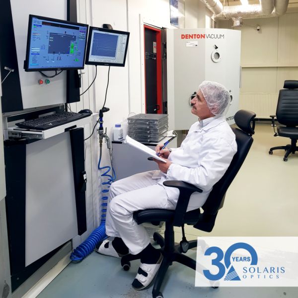
Figure 1 Mr Zdzislaw Choromanski in Optical Thin Film Facility
What was the process of making thin layers in Poland in the 90s?
The method is still similar, but back then there was a lack of ion-assisted technology, modern monitoring devices and digital process control, to name a few main differences. There were a few centers on the market with quite primitive devices. Competitiveness largely depended on the innovation of the mastered technology.
If there were no monitoring devices to control the process, how was it done? What are the benefits of implementing these techniques?
Today we have a monochromator [an optical device used to study characteristics of optical filters], while those times we had to use various types of commercial filters. Their quality and stability left much to be desired. So, the monochormator was a big step forward.
The way quartz systems are used to control thickness and speed of layer deposition has also changed. These systems are based on a piezoelectric quartz plate, which is covered with electrodes. The resonant frequency of such a system depends on its mass, i.e. what and how much was deposited on it. If the coating is vaporized, the vibration frequency of the resonator depends on the mass of the deposited material – if we can control the change in the frequency of vibrations and we know the material density, we can determine the thickness of the deposited layer and the rate of application (e.g. nm / min). In the past, the deposition process was controlled in this way, today it is an automated process. Similarly, today these systems scale themselves, and in the past you had to do it manually.
How would you rate the advancement level of thin film technology in Poland today?
Currently, few centers in Poland have modern thin-film technology. Actually, only Solaris Optics offers its commercial use on a large scale. The others are mainly industry and academic centers. I think we are highly competitive in the global market, at least in the PVD EB PIAD application area.
Looking at the history of the development of thin film technology, what direction are we going in your opinion?
I believe that in parallel with the development and extension of existing methods such as IBAD and PIAD to the PVD EB, new coating methods will continue to be developed, as IBS was born. Each of these methods will evolve towards increasing accuracy and increasing other parameters.
Looking historically and starting with a simple vaporization. It was initially a thermal process, then an Electron Beam Gun was added to it, which extended the possibility of vaporization of new, previously unavailable materials. Over time, ionic techniques have come, the use of a reactive and energy-assisted process, in which the ions hand over energy, and the resulting layer is more stoichiometric [properly oxygenated, which improves its properties], better packed. Ion support also takes many forms, such as IBAD, PIAD that we use as well and other techniques. This is the evolution of just one method.
Apart from that, other methods are being created and developed, such as sputtering, where we have a target, voltage, ionization of the neutral gas, which knocks out particles from the target. Those particles are later deposited on the element. A further development is, for example, Ion Beam Sputtering, in which the device acts not on the target, but on the coated element.
Additionally we have CVD, in which the particles from the gas phase react to form a layer on the element. This is an example of a method for creating e.g. diamond-like carbon layers. Such layers which fulfill mechanical tasks, but also function optically. Another method is spin coating, in which a sol-gel suspension is spread by centrifugal force on a rotating element and becomes gelled.
In addition to the development of the methods themselves, the aim is to expand the materials used, which provide new opportunities. We mainly use oxides and fluorides. Recently, nitrides have been gaining popularity, also in optical applications, e.g. for reflecting thin film coatings with high chemical and mechanical resistance.
Coming back to your department – what is the potential of Solaris Optics in the field of thin films, what kind of inquiries do you handle and for which clients?
Solaris Optics has three devices for applying optical thin-film coatings. We basically offer a full range of coating types that can be applied with the PVD EB IAD and PIAD methods. These coatings can operate in spectral ranges from ultraviolet (248 nm) to mid-infrared (5 micrometers). We coat optical elements with dimensions ranging from 3 to 300 mm in diameter.
If you would be asked for an example of a custom and interesting thin-film coating challenge, what would it be?
There were many challenges, but the development of the LVGF [Linear Variable Gradient Filter] production technology was extremely spectacular, where the method based on a non-standard idea gave an interesting result. The filter was used in the Sentinel-5 project, probably in a spectrophotometric system.
One of your colleagues described making optical thin-film coatings as a process with a certain element of art in it. What do you think about this opinion?
There is something to it… The enormous number of variables that influence the result of the coating process makes it quite complicated. For example, the geometry of the vaporization system, its repeatability, temperature, the speed of deposition of the layers, the presence and use of reactive and inert gases in the process, etc. From the outside it looks very complicated… After getting into the topic, one starts to understand it, but it takes time. Hence, a kind of intuition is needed, obviously resulting from experience and understanding the essence of the process.
Mr Choromanski, thank you very much for the interview.
***
