Spherical Plano Lenses, Mirrors, Windows – Faster with Improved Quality with Diamond-pallet Grinding

Published: January 5, 2023

A shorter lead time is perhaps the third most important criterion (two others are capabilities and price) when it comes to ordering custom optics products, such as mirrors, windows, blanks, lenses (also spherical plano lenses) and prisms. In some market situations, such as we observe in 2021 and 2022, the lead time prevails over price.

Solaris Optics, a manufacturer of precision optics elements, finds shortening lead time as one of priority development areas, next to quality and technical capabilities. In the following article we refer to findings from our recent investment in new grinding capabilities.

New Grinding Technique for Improved Quality

With technical capabilities, quality and lead time development as the main goals, Solaris embarked on an investment project aimed at development of R&D infrastructure, back in 2019. The project assumed purchases of various equipment, including one-sided automated grinders along with a set of diamond pallets. The project resulted in several R&D projects and developments in Solaris Optics, as described in detail in our earlier publications, such as Subsurface Damages Reduction for Precise Optics Manufacturing or Raster Mode to Expand Capabilities of Magnetorheological Finishing.

In regards to automated grinding with diamond palettes, Solaris Optics engineers assumed that adding the method to company manufacturing portfolio will allow to speed up optical grinding and polishing phases. The shorter process time shall be possible by higher efficiency of grinding, but also by keeping the subsurface damages minimized, which shall allow to reduce the polishing time needed to reach the required surface quality of optical elements.

The machine was turned into use in 2021 and quickly proved the reduction of sub-surface damages.
Then it was further tested to understand how the new process can affect the overall manufacturing speed. As explained in the aforementioned article it was expected that “the main benefits for clients include shorter lead times and lower costs with improved final product quality (i.e. less scatter, better durability).” After about 1.5 years after implementation we can announce some conclusions from the investment.

Spherical Plano Lenses – Surface Process Time Down by 40%

Our technology team tested and compared production times of 11 different optical products using a traditional process and a new one, which included the new grinding method. The tested products were of various sizes, materials and types, such as spherical plano lenses, mirror substrates, optical windows and filters. Materials included e.g. borosilicate crown glass, crown type Soda lime glass, Quarz and filter glass.
With the new technique the team managed to significantly speed up the grinding times, whereas the overall gain on grinding + polishing time was reduced by over 42% on average (37% to almost 50%), with many dependencies between product characteristics and processing time uncovered. The exercise proved not only the efficiency of grinding with diamond-based pallets, but also that, there is shorter polishing time needed due to reduction of sub-surface damages at the earlier stage.

Higher Speed, Quality and Increased Competitiveness

The investment in automated grinding with diamond palettes proved successful in the assumed goals, i.e. shortening lead times and improving product quality. Apart from the tested product types, i.e. windows, mirror substrates, filters and sphetical plano lenses, the technology process and it’s gains are applicable also to other precision plano optical elements as well as to prisms.
The new production machinery enables further improvement of Solaris Optics competitiveness and the existing clients already benefit from the advantages. In the future Solaris plans to complement the technique with spherical grinding possibilities.

Should you be interested to cooperate with Solaris Optics, please do not hesitate to contact us.

The diamond grinding investment is a part of a project titled Development of R&D infrastructure of Solaris Optics S.A. as a way to implement innovation, realized by Solaris Optics with financial support from the European Regional Development Fund under the Regional Operational Program of the Mazowieckie Voivodeship for 2014-2020, Sub-measure 1.2. Research and development activities of enterprises.

Optical Materials for Medical NIR Applications

Published: November 2, 2022

Medical infrared (IR) applications refer to the use of infrared light for various healthcare purposes. It includes such medical domains as surgery, skin treatment, spectroscopy or thermography.

Optical spectrum is, in general, divided into: ultraviolet (UV), visible (VIS) and infrared (IR) radiation. Nevertheless, especially for the infrared spectrum, due to many practical and application reasons, the spectrum is further split into:

  • Near infrared: 0.75 – 1.0 um (sometimes defined up to 2.5um)
  • Short infrared radiation: 1 – 2.5 um
  • Medium infrared radiation: 3 – 5 um
  • Long infrared radiation: 8 – 12 um

In the following article we focused on some typical near-infrared (NIR) applications for medical purposes and the most commonly selected optical materials for those.

Optical Material Selection for Medical NIR

The process and criteria of optical material selection are a part of a wider discipline of equipment design. Hence, the selected material must fit the general and specific purposes of the equipment to be conceived.

Medical devices, from the application engineering perspective, shall be seen as laboratory-level instruments, given they are used in hospitals, health centers, clinics or aesthetic medicine centers. Such locations are distinguished by well defined and almost stable work environment – lack of shocks, clean surroundings, low fluctuations of temperature. Such devices are predominantly used by trained and qualified personnel.

Laboratory-level working conditions are perhaps the most advantageous from design perspective. They allow to focus on equipment performance parameters, manufacturability, price optimization, ergonomics, etc. They typically do not put any relevant non-standard requirements on optical materials to be used.

Medical Applications of NIR

In absence of major external factors affecting the choice of optical materials, the engineer can focus on the optical matters, i.e. suitability of the optical setup to the given task. The main questions are related to the application itself (e.g. is it related to imaging, lighting, laser beam control) and specification of the required optical system, as well as the wavelengths and power of light.

Within the NIR a review of available publications, shows two main directions, where the NIR spectrum is of use in healthcare: human tissue interaction and NIR spectrometry.

Optical Materials for Laser-Tissue Interaction

The type of interaction of laser light with human skin is diverse and includes: transmission, reflection, scattering and absorption. In majority of cases the most relevant phenomena is absorption, as it effectively transfers the photon energy to tissues. NIR wavelengths are proven very effective in many applications related to human tissue.

The laser-skin interaction can be in simple terms described as depending on the wavelength applied so that the longer the wavelength the deeper into the skin it can reach. This enables applications on the skin surface as well as under the skin, including e.g. hair removal (~700nm), wound healing (e.g. 890 nm), tattoo removal (various visible and NIR wavelengths such as 1064 nm, depending on ink color), vein treatment, hemostasis or tumor necrosis (1064 nm). As listed, depending on specific case a different wavelength is advantageous and within the range the typical laser sources include e.g. Nd:YAG (1064 nm), Alexandrite laser (755 nm), diode lasers (~800-900 nm) or Ruby laser (694 nm).

The above wavelengths are crucial in defining the actual optical material to be used. Fortunately for the given ranges, some common VIS transparent materials, such as optical glass, e.g. N-BK7, Fused Silica or IR Fused Silica show also transparency within NIR spectrum. Hence, they are suitable as materials for optical components, such as lenses and optical windows.

Schott N-BK7 transmittance curve for 10 mm glass thickness
Figure 1 Schott N-BK7 transmittance curve for 10 mm glass thickness


Optical Materials for NIR Spectrometry

Spectrometry is an analytical method based on interaction between electromagnetic radiation, such as laser light, and a matter. It is applied to study the contents of materials, molecules of various compounds. In spectroscopy the NIR spectrum range is often defined a bit wider than mentioned above, e.g. from 700 nm to 2500 nm. NIR spectroscopy finds applications for material analysis in pharmaceutical, chemical, food, agricultural and healthcare sectors.

For healthcare applications the NIR range is advantageous as its absorption by water and hemoglobin is minimal, which opens a possibility to study other compounds and diagnose diseases. Some medical uses of NIR spectroscopy include blood testing, identification of proteins or noninvasive monitoring.

For spectroscopic applications, where the NIR is sampled along the spectrum it is relevant to ensure that the optical materials guarantee high and even transmission (lenses, windows, prisms) or reflection (mirrors) along the spectrum. Hence example optical glasses include IR grade Fused Silica, Calcium Fluoride CaF2, Magnesium Fluoride MgF2 or Silicon.

Internal Transmittance Calcium Fluoride from OHARA
Figure 2 Internal Transmittance Calcium Fluoride from OHARA

Optical Materials for NIR Medical Applications

Medical NIR applications include mainly non-imaging laser uses. In such cases we have typically rather simple optical setups, which makes optical material selection a bit easier. Materials indicated above, such as N-BK7, Fused Silica, Calcium Fluoride, Silicon and others belong to the “mainstream” of optical materials, used commonly in many applications. It shall be remembered however, that optical elements are usually additionally coated, at least with an AR layer, which comprises of another type of optical materials used in medical NIR applications and was not covered in the article.

Solaris Optics manufactures components, including planar, spherical, mild-aspherical, from all of the above mentioned optical glasses and crystals. We do also thin film design and deposition, and we have experience in the manufacture of optics for medical applications. Should you be interested to learn more, please do not hesitate to contact us.


Custom Optics Manufacture vs Catalogue Optics

Published: August 12, 2022

Custom optics manufacture means the production of optical components, such as lenses, prisms, mirrors, etc. according to customer specifications, technical or application guidelines or other specific requirements.
Catalogue optics or off-the-shelf optics, compared to custom optics, are products that are purchased with predefined characteristics, where the customer shall take into consideration the specifications provided by the supplier.

We at Solaris Optics receive many inquiries regarding catalogue cards of products we manufacture. Such questions typically open the discussion about technical capabilities, however we realised that it is needed to explain the main differences between a catalogue supplier and a custom optics manufacturer. Hence we drafted an article to explain in more detail what to expect and what not to expect from a custom optics manufacturer. The contents have a form of discussion of the main advantages and disadvantages of catalogue and custom optics suppliers.

Custom optics manufacture – pros & cons

Both custom optics producers as well as catalogue optics suppliers complement each other and are successfully operating on the market. Some of the most known catalogue optics suppliers include e.g. Edmund Optics or Thorlabs, whereas a good example of a custom optics manufacturer is Solaris Optics.

Video presenting overview of Solaris Optics manufacturing steps and processes: Continue reading below the video.
 

There are several good reasons to order optics from a producer of bespoke optics. The main advantages
include:

  • More flexibility when it comes to specifications – typically within its range of technical capabilities a custom optics manufacturer is flexible when it comes to its offered products, hence any inquiry within the manufacturing limits is a usual client case. Naturally one can never say that there are no limits when it comes to available specifications from a custom optics manufacturer. Any optics producer has its technical manufacturing limits which set the boundaries of what can be practically done – what materials and shapes can be processed, what thin film coatings can be deposited and what shapes, dimensions and surfaces can be measured.
  • Own manufacturing facilities – typically a custom optics manufacturer is distinguished with its own production space, where the ordered products are manufactured; this allows clients to personally verify the production standards whenever needed, but also allows the manufacturer to adjust certain production standards for a given client when needed. This becomes especially relevant in the changing supplier paradigm, where the manufacturing is expected to be local or near as opposed to distant and price-prioritised.
  • Economic competitiveness with increasing volumes – with lower volumes devoted optics producers are not able to compete against catalogue suppliers with a price. However, with larger volumes the cost structure of production and sales gets advantageous for optical components manufacturers; no intermediaries, as well as organisations, focused on production rather than sales & marketing allow the custom optics manufacturers to be fully competitive with price versus catalogue products.

Custom optics manufacturer, Solaris Optics
Figure 1 Custom optics manufacture at Solaris Optics

The business characteristics of a custom optics producer brings, however, certain features, which can be seen as disadvantageous:

  • Longer lead times – the necessity to process the inquiry, plan production, order substrates, manufacture and measure, makes it impossible for a custom optics producer to match the delivery times of catalogued products.
  • Limited possibility to manufacture small volumes – some custom optics manufacturers may find it difficult to execute small orders, such as 1, 5 or 10 pieces; such orders are usually a domain of off-the-shelf suppliers, as long as the predefined specs are suitable.
  • For small volumes higher production costs – with new product manufacture there are several costs to bear, e.g. design and purchase of product-specific tools for glass processing; when the volume is small, the production may come up uneconomical.

Catalogue optics – pros & cons

The advantages and disadvantages of catalogue optics as compared to custom optics are naturally mirroring each other.
Main advantages of catalogue optics:

  • Typically short lead time – usually the catalogue parts are available in stock, ready to send, so it is possible to get the needed parts within e.g. 3-4 days.
  • The possibility to order a single piece, but also larger volumes – the critical factor is oftentimes the possibility to order small amounts, e.g. 1, 5, 10 pieces, which is either not possible or costly from custom optics manufacturers; for higher volumes the situation may be a bit more complicated, as it may require production re-planning, so similar activities as typical custom optics manufacturers do
  • Competitive price, especially at low volumes – while it takes several preparation steps to plan and execute a production process for a given component, for catalogue suppliers, all those steps are not necessary.

Nevertheless, some disadvantages of catalogue optics vendors include:

  • Limited specifications – it is possible to utilise the above-mentioned advantages as long as the product design assumptions can be adjusted to the already existing predefined specs in the supplier offer; this means component selection with optics catalogue and compromising on e.g. dimensions, spectral characteristics of the optical element or on the entire product final size and performance. Usually, catalogue optics suppliers try to adapt their warehouse offer to the most common market requirements, but this is not always possible.
  • Unknown manufacturer – in many cases a catalogue optics supplier is actually a company that organises supplies and arranges sales, but is not a manufacturer itself; hence it has limited possibilities, or at least a longer way, to adjust the production to some specific requirements; this is oftentimes relevant when a customer seeks to place a larger order.
  • Limited price competitiveness at larger volumes – with larger volumes the price advantage of catalogue suppliers starts to disappear, and the price can be higher as compared to an offer from a custom optics manufacturer.
  • Limited flexibility – certain clients are interested to adjust not only the production process but also certain supplier operations standards; for a catalogue supplier, this may be either impossible or difficult to adhere to.

Custom optics or catalogue optics

Given the above brief analysis, there are several conclusions that can be drawn.

It is clear that as long as the developed optical product is of low volume or in the prototyping phase – it is economically advantageous to select a catalogue supplier for minimum costs and quick delivery. When the needed product is of higher volumes then it is good to ask for offers also from custom optics producers. For high-volume products, where the specs are beyond catalogue-available specifications it is likely that devoted optics suppliers will provide you with better offers and more flexibility than off-the-shelf suppliers.

While the above conclusions are in a majority of cases true, there are also other cases, where the answer is not obvious and the supplier selection will be case-specific. For instance, an order for 50-100 components can be economic from both a catalogue and a custom optics supplier. Perhaps in the most challenging situation are scientists or product developers who develop products which cannot accept compromises on optics specs. In such a case a custom optics supplier which: A – has the needed capabilities and B – has a suitable business situation to handle the inquiry shall be sought.

In the above article, we tried to explain the main differences between the two business models: catalogue supply and custom manufacture, looking from a customer perspective. We trust that with the time spent on reading the publication you will now save time on optics supplier or manufacturer selection. Should your choice be a custom optics manufacturer, kindly please consider Solaris Optics.

Solaris Optics is a custom optics manufacturer, based near Warsaw in Poland. We are happy to answer your questions!

Please follow us also on Linkedin, Facebook and Youtube!

***

SWIR Lenses and SWIR Filters for Earth Observation Small Satellite for Maritime Surveillance

Published: June 23, 2022

SWIR lenses and SWIR filters shall be studied, designed and prototyped in another space-related project, in which Solaris Optics participates.

By the end of 2021 Solaris Optics confirmed its participation in an EU-funded project with a working title Novel Earth and Maritime Observation Satellite, acronymed NEMOS. The project is realized under the European Defence Industrial Development Programme (EDIDP) 2020, within the topic: Multifunctional capabilities, including space based surveillance and tracking, able to enhance the maritime awareness (discover, locate, identify, classify and counteract the threats).

The NEMOS consortium is led by SATLANTIS MICROSATS S.L. a Spanish expert in very high-resolution optical payloads for Earth observation small satellites. The ultimate goal of the initiative is to design a small optical satellite for Low Earth Orbit, which will ensure high resolution imaging of maritime littoral, high sea areas, harbour and critical infrastructure for quasi real-time intelligence, surveillance and reconnaissance. Solaris Optics is one of eleven consortium members and the only one from CEE region.

SWIR Filters and SWIR Lenses Manufacture

The role of Solaris Optics, a precision optics manufacturer, in the project includes development of production and measurement methodologies to enable manufacturing of optical elements for the space telescopes.
The early-assumed spectral ranges for the optics are within very near infrared VNIR 450 – 900 nm and another for short-wave infrared SWIR 900 – 1700 nm, however further studies will allow to draw final specifications for the VNIR and SWIR lenses and filters.

The tasks include optical lens system feasibility study and analysis, as well as similar studies about the needed optical filters and thin film coatings. The coatings of various types, including reflective, anti-reflective and filters will be studied and designed for the assumed spectral ranges. With a goal of high quality imaging of the final system, the manufacturing process shall ensure high precision of optical elements, with assumed use of Solaris Optics state of art technologies, including MRF technology, for example.

NEMOS Participants, SWIR lenses and filters
Figure 1 NEMOS Project participants

Optics for Space Imaging

Solaris Optics continues its development within precision optics manufacturing, which is especially beneficial for space imaging applications. For the maritime observation satellite Solaris Optics will utilize its previous experiences in the matter, such as the development of Earth observation optical system, a project realized in cooperation with the European Space Agency, where Solaris took a leading role.

NEMOS Schedule and Funding

The European Defence Industrial Development Programme is the first ever EU funding programme aimed to co-finance the development of defence solutions in collaborative projects. In 2020 the EU allocated 158.3 m EUR to 26 projects under EDIDP, including NEMOS. The NEMOS project has a duration of 24 months. The total contribution of the EU funding to NEMOS is 3 983 001.68 EUR.

To learn more about very high resolution optical payloads for small satellites, please contact SATLANTIS MICROSATS S.L.

Should you have questions regarding Solaris Optics capabilities for space imaging, please do not hesitate to contact us!

***

Spectrometer Prism – Typical Designs

Published: May 9, 2022

Spectrometer prism is a core enabling element of optical spectrometry, which deals with wavelength spectrum analysis. An optical spectrometer deploys a dispersive element – a prism or a diffraction grating, to break down the incoming light into its wavelength components. Modern spectrometers provide high resolution and accuracy in frequency and time domains, operate in a wide spectrum and provide a basis for many modern optical applications in pharmaceutics, food testing, space observation and much more.
 
In this article we present an overview of main spectrometer prisms – typical prism designs used for optical spectrometry.
 
The prism was traditionally used for the light dispersion purposes in spectrometry, while the introduction of diffraction gratings and the subsequent development of their quality and efficiency have contributed to their increasing popularity. Nowadays, prisms are still widely used in the low-light applications where inferior transmission of gratings tend to be a blocking point. In such demanding scenarios, prisms exceed diffraction gratings in terms of sensitivity and signal-to-noise ratio. While prism-based spectrometers can offer light throughput efficiency exceeding 90%, diffraction gratings typically offer efficiency of below 70%.

Prism in Spectrometry

Prism are the original dispersion elements used in optics and their use in spectrometry can be dated back to 18th century and works of Sir Isaac Newton.
 

Spectrometer prism - dispersion basics
Figure 1 Prism-based Light Dispersion Basics

Prism is a solid structure made from transparent optical material with non-parallel end faces resulting in dispersing of the passing light into its constituent wavelengths. As a result, it is possible to examine the distribution of wavelength in the incident light. Developments in materials and designs have allowed to tackle many limitations of prisms, such as non-linear dispersion, efficiency, UV absorption or thermal stability. Nowadays, optical engineers have a wide choice of prism geometries and materials that offer unique properties and functionalities to match the desired specification.

Spectrometer Prism Geometries

Selecting the optimal prism geometry for the setup involves considering several factors. The geometry and material of the prism have an important effect on their performance, most notably the total deflection angle and linear dispersion at the detection plane.
 
The most basic type of spectrometer involves an equilateral prism consisting of three equal 60° angles. The dispersion of such prism is a function of its geometry and refractive index. As the refraction coefficient n of optical material depends on wavelength, individual components of a non-monochromatic beam are distinctively refracted by prism’s entrance and exit surfaces and their paths are changed accordingly. As a result, each monochromatic beam will be refracted by a specific angle from its original direction. Many modern prism spectrometers usually use prisms in series to address dispersion in the optical system and enhance the angular spread of the beam.
 
The alternative is an uncoated Littrow prism, typically a 30°-60°-90° prism which is easier to manufacture but offer a narrower dispersion range. The design takes advantage of the arrangement in which the light entering the element at the Brewster angle experiences a strong dispersion.
 
Another example is an objective prism, which is defined by a small apex angle but a large size. Its inherent advantage is a wide field, making it possible e.g. in space observation to capture the spectrum of large number of stars at the same time.

Materials of Spectrometer Prisms

The choice of dispersive material is as important as prism geometry when designing a spectrometer. The material needs to exhibit strong change of refraction indexes across different wavelengths. Also, selecting the optimal material depends heavily on the spectrum to be measured. Optical glasses such as BK7 or flint glasses usually cover the complete visible range, while the common IR-compatible materials are zinc selenide, germanium or silicon. For the measurements in UV range, fused silica or quartz prisms are mostly deployed. Additional anti-reflective coatings can enhance performance of the prism in the desired spectrum region.

Manufacturing of a Spectrometer Prism

Since their discovery dispersion prisms have been widely used to split light into its spectral components and thanks to their efficiency and broad bandwidth are still relevant in the field of spectrometry. Please note the quality of a spectrometric system will largely depend on the quality of the components used. Manufacturing of high-precision prisms to be used in spectrometry demands strict tolerances and accuracies. New technologies, such as Magneto Rheological Finishing (MRF) allow to produce exceptionally smooth optical surfaces with figure error as low as ~1 nm RMS.
 
Solaris Optics manufactures various prisms in its manufacturing facilities near Warsaw in Poland. Please contact us if you wish to learn more about high-performance prism manufacturing capabilities of Solaris Optics.

***

Solaris Optics CEO on Company History, Presence and Future

Published: February 28, 2022

Precision Optics Manufacturer Outlines its Post-Pandemic Future” – it’s a title of a longer interview made by Jose Pozo, the CTO of EPIC Photonics Association, with the CEO of Solaris Optics, Michal Muniak. Solaris Optics joined EPIC Photonics Association in early 2021. The interview was published at novuslight.com, in the second half of February 2022 and it covers the CEO personal and company takes on Solaris Optics.

The publication summarizes a bunch of interesting facts about Solaris Optics development, markets and plans, which we outline below.

Main development milestones in the company history:

  • 1991 – founded, Philips as the first significant customer,
  • 2000 – own manufacturing premises in Józefów n. Warsaw including 1620 sqm of production spaces,
  • 2005 – ISO 9001 certification for optical components manufacture and assembly,
  • 2012 – set up of own R&D group to provide high-level engineering services in optics,
  • 2015 – significant investment in production and measurement equipment, including MRF polishing machine, first of this kind in CEE.

Company status and capabilities as of 2022:

  • employment: 70
  • product capabilities: lenses, filters, mirrors, polarizers, prisms, beamsplitters, diffusers, electro-optic modulators; optics tuned for imaging, infrared and laser applications
  • optical materials processed: all types of optical glasses, quartz glasses, optical ceramics and crystal;
  • services: manufacturing (cutting. milling, grinding, polishing and high-precision finishing), optical design, thin-film coatings and metrology.

Markets:

  • Main application sectors of Solaris Optics products include: semiconductor industry, material processing, telecommunications, lithography, imaging, and scientific research, space and defence.
  • Exports – about 95% of total production is exported, with main target markets such as Germany, Netherlands, Taiwan and Israel.

Michal Muniak on Solaris Optics future:

  • Solaris Optics currently finalizes its’ 5-year strategy aiming improvements in several areas, i.e. effective commercialization, custom optics, free-form optics applications
  • commercialization – the focus is to shift the company from scientific, oftentimes niche applications towards selected segments and more specialized production
  • custom optics – the aim is to be able to quickly provide full range of custom optics services, from prototype development to full scale, volume production
  • free-form optics applications – utilization and development of novel manufacturing techniques, such as MRF, as well as new measurement methods in order to satisfy a new market demand for free form optics.

Asked about advice for entrepreneurs Mr Muniak underlined the importance of people he works with and suggested to find ways to “go outside your bubble”!

For full interview please visit Precision Optics Manufacturer Outlines its Post-Pandemic Future.

***

Optical Contact Bonding Capabilities in Solaris Optics

Published: January 31, 2022

Optical contact bonding is a technique, in which two optical elements are joined with no additional bonding component, in particular – no chemical adhesives. The bonding process takes place on a molecular level.

In the following article we describe the capabilities and limits of optical contact bonding in Solaris Optics. Before we go further, for the readers who have not read our publication on optical bonding, a brief reminder.
There are several significant advantages related to the lack of adhesive in element bonding, including:

  • cleanliness of the bonded optical element; for applications in vacuum environments such adhesives can e.g. contaminate the optical surfaces, whereas with contact bonding such issues disappear;
  • no additional refractive index along the optical path; this is advantageous for instance in some demanding measurement applications. With a proper material selection (e.g. glasses from the same melt) a bonded component performs optically almost like a single optical component (although typically some reflections may occur).

Contact Bonding in Production

Solaris Optics uses optical contact bonding technique regularly in its production processes, for fine grinding and polishing of components. In an example case, a set of prisms to be grinded, instead of traditional gluing, is contact-bonded on a grinding shawl. The obtained contact joint is strong enough to withstand the shear force in the grinding or polishing processes. With such experiences Solaris Optics started to investigate and use the optical contact bonding technique also for regular component manufacturing.
The method can be applied to any bonding, where two surfaces to be joined are flat. So the optical components potentially prone for contact bonding include: prisms and beam splitters, wedges, filters and optical windows, lenses as well as special combinations, e.g. a prism joined with a diffraction grating, or a filter bonded with a microlens array.

Prerequisites for Optical Contact Bonding of Components

The first and most relevant technical requirement is, as mentioned already, the flatness of the surfaces to be joined, i.e. each element to be joined must have at least one polished flat surface. Specifically the flatness:

  • for overall dimensions < 60 mm shall be better than 3/0,5(0,5)
  • for overall dimensions of more than 60 mm and less than 170 mm the flatness be better than 3/1(0,5).

With the above flatness parameters Solaris Optics is able to achieve the intermolecular adhesion between the optical surfaces. Solaris Optics offers polishing capabilities required to reach the expected flatness, however it is also theoretically possible that the elements with such flatness are can be delivered by the client. In such cases an additional testing at Solaris laboratories will be necessary. Solaris Optics does not offer contact bonding for non-flat surfaces.

Optical Contact Bonding Process
Figure 1 Optical Contact Bonding Process

Dimensional Limitations for Contact Bonding

Depending on the type of the element, the range of dimensions of the surfaces to be joined varies. Max overall dimensions for specific elements are as follows:

  • windows – up to 170 mm
  • wedges – up to 100 mm
  • prisms – up to 60 mm
  • filters – up to 100 mm
  • plano-concave lenses – up to 100 mm
  • plano–convex lenses – up to 100 mm

Other elements or elements outside the above dimensions – shall be considered individually.

Optical Contact Bonding - Removing Air
Figure 2 Optical Contact Bonding Process- Removing Air

Optical Materials for Optical Contact Bonding

Solaris Optics can bond the following materials: N-BK7, UV fused silica, magnesium fluoride (MgF2) silicon and germanium. We do not offer contact joining for calcium fluoride (CaF2), nor for zinc selenide (ZnSe) or other environmentally hazardous glasses. If components shall be connected via optical contact, the materials shall be carefully planned during the design stage, especially when different materials will be fixed. Moisture, temperature effects, in cases where the heat is generated either by illumination or in the working environment, shall be taken into consideration.
Solaris Optics secures the optical contact bond against moisture via lacquering technique. We have not tested the influence of temperature on the various combinations of optical bonds, though. Hence any cooperation shall be preceded by manufacturing tests.

Thin Film Coatings in Contact Bonding

Can thin film coated surfaces be contact-bonded? The answer is ambiguous. According to our main technologist, typically AR-coated surfaces can be joined with optical contact. Other thin film materials, shall be considered case by case, so please share your inquiry with us, to learn our capabilities for the given case.

Summary and Challenges

Optical contact bonding may find applications e.g. in medical, aerospace or scientific domains, where either the gaseous contamination or optical path disturbance caused by adhesives shall be avoided.
When designing for optical contact bonding, similar factors as with regular cement bonding shall be taken into consideration. Risks of de-bonding may be related to i.e. e.g. working and environment conditions, such as mechanical shock, vibrations, temperature fluctuation, or moisture.
 
Solaris Optics engineers are available for discussing specific issues related to optical contact bonding, either at the design or manufacturing stage.

***

30 Years in Optical Thin Film Coatings Development – Interview

Published: December 30, 2021

Interview with Mr Zdzisław Choromański, Head of Optical Thin Films Department as Solaris Optics

Mr Zdzisław Choromański is one of the first employees of Solaris Optics, in 2021 celebrating the anniversary of 30 years of employment in the company. Since the beginning Mr Choromanski has been responsible for optical thin film deposition processes, the department developments and investments. In the interview Mr Choromański shares his perspecitves about the history and future of optical thin film development, as well as about the advancement of his department in Solaris Optics.

Mr. Choromanski, you joined Solaris Optics 30 years ago, shortly after the company was founded. Please accept congratulations on the 30th anniversary of work.

Thank you very much.

Could you go back and tell readers what life was like at that time?

A bit like today, but many techniques were missing, mainly communication and digital, which we now take for granted. But it was a period of rapid development of those technologies, so our task was to learn and put into use everything that was useful.

What was the company like when you joined?

About 20 employees, one vacuum sputtering machine, tight spaces. But every day we learned something new and improved our work. With time, a new headquarters was established, we introduced new coating equipment, and the number of employees has been constantly growing.

Who was the first significant customer of the company?

It is difficult to say who was the first important customer of the company – at the beginning we had many small customers, which meant that the variety of work, both then and now, is very large. Later, in the 2000s, a large manufacturer of laser devices became our key customer.

Today you are the head of the thin film technology department and a recognized expert in this field in Poland. What position did you come to for Solaris, what did you do before?

I have been with Solaris Optics from the very beginning. I organized thin-film coating from scratch. After studying at the Warsaw University of Technology, I worked at the Institute of Plasma Physics and Laser Microfusion, where I learned the ins and outs of thin-film coating and an innovative approach to work. Most of the first Solaris Optics employees come from the Institute.

Optical thin film coatings
Figure 1 Mr Zdzislaw Choromanski in Optical Thin Film Facility

What was the process of making thin layers in Poland in the 90s?

The method is still similar, but back then there was a lack of ion-assisted technology, modern monitoring devices and digital process control, to name a few main differences. There were a few centers on the market with quite primitive devices. Competitiveness largely depended on the innovation of the mastered technology.

If there were no monitoring devices to control the process, how was it done? What are the benefits of implementing these techniques?

Today we have a monochromator [an optical device used to study characteristics of optical filters], while those times we had to use various types of commercial filters. Their quality and stability left much to be desired. So, the monochormator was a big step forward.

The way quartz systems are used to control thickness and speed of layer deposition has also changed. These systems are based on a piezoelectric quartz plate, which is covered with electrodes. The resonant frequency of such a system depends on its mass, i.e. what and how much was deposited on it. If the coating is vaporized, the vibration frequency of the resonator depends on the mass of the deposited material – if we can control the change in the frequency of vibrations and we know the material density, we can determine the thickness of the deposited layer and the rate of application (e.g. nm / min). In the past, the deposition process was controlled in this way, today it is an automated process. Similarly, today these systems scale themselves, and in the past you had to do it manually.

How would you rate the advancement level of thin film technology in Poland today?

Currently, few centers in Poland have modern thin-film technology. Actually, only Solaris Optics offers its commercial use on a large scale. The others are mainly industry and academic centers. I think we are highly competitive in the global market, at least in the PVD EB PIAD application area.

Looking at the history of the development of thin film technology, what direction are we going in your opinion?

I believe that in parallel with the development and extension of existing methods such as IBAD and PIAD to the PVD EB, new coating methods will continue to be developed, as IBS was born. Each of these methods will evolve towards increasing accuracy and increasing other parameters.

Looking historically and starting with a simple vaporization.  It was initially a thermal process, then an Electron Beam Gun was added to it, which extended the possibility of vaporization of new, previously unavailable materials. Over time, ionic techniques have come, the use of a reactive and energy-assisted process, in which the ions hand over energy, and the resulting layer is more stoichiometric [properly oxygenated, which improves its properties], better packed. Ion support also takes many forms, such as IBAD, PIAD that we use as well and other techniques. This is the evolution of just one method.

Apart from that, other methods are being created and developed, such as sputtering, where we have a target, voltage, ionization of the neutral gas, which knocks out particles from the target. Those particles are later deposited on the element. A further development is, for example, Ion Beam Sputtering, in which the device acts not on the target, but on the coated element.

Additionally we have CVD, in which the particles from the gas phase react to form a layer on the element. This is an example of a method for creating e.g. diamond-like carbon layers. Such layers which fulfill mechanical tasks, but also function optically. Another method is spin coating, in which a sol-gel suspension is spread by centrifugal force on a rotating element and becomes gelled.

In addition to the development of the methods themselves, the aim is to expand the materials used, which provide new opportunities. We mainly use oxides and fluorides. Recently, nitrides have been gaining popularity, also in optical applications, e.g. for reflecting thin film coatings with high chemical and mechanical resistance.

Coming back to your department – what is the potential of Solaris Optics in the field of thin films, what kind of inquiries do you handle and for which clients?

Solaris Optics has three devices for applying optical thin-film coatings. We basically offer a full range of coating types that can be applied with the PVD EB IAD and PIAD methods. These coatings can operate in spectral ranges from ultraviolet (248 nm) to mid-infrared (5 micrometers). We coat optical elements with dimensions ranging from 3 to 300 mm in diameter.

If you would be asked for an example of a custom and interesting thin-film coating challenge, what would it be?

There were many challenges, but the development of the LVGF [Linear Variable Gradient Filter] production technology was extremely spectacular, where the method based on a non-standard idea gave an interesting result. The filter was used in the Sentinel-5 project, probably in a spectrophotometric system.

One of your colleagues described making optical thin-film coatings as a process with a certain element of art in it. What do you think about this opinion?

There is something to it… The enormous number of variables that influence the result of the coating process makes it quite complicated. For example, the geometry of the vaporization system, its repeatability, temperature, the speed of deposition of the layers, the presence and use of reactive and inert gases in the process, etc. From the outside it looks very complicated… After getting into the topic, one starts to understand it, but it takes time. Hence, a kind of intuition is needed, obviously resulting from experience and understanding the essence of the process.

Mr Choromanski, thank you very much for the interview.

***

Raster Mode to Expand Capabilities of Magneto-Rheological Finishing

Published: November 26, 2021

QED Q-flex 300 Magneto-Rheological Finishing (MRF) system has been used by Solaris Optics S.A. since 2015 and during this time proven to be able to produce optics with accuracy and precision unmatched by many competing technologies. The recent addition of a Raster Module is a further development towards higher precision of optical surfaces, by allowing to correct drawbacks of a rotational mode.

Magnetorheological polishing is a deterministic method for precise treatment of crystalline and glass optical surfaces which uses a fluid consisting of a polishing agent, magnetizable particles and stabilizing additives to perform material removal.

MRF Rotational Polishing Mode
Figure 1 MRF Rotational Polishing Mode

The fluid is applied by a nozzle on a rotating wheel and a stable polishing ribbon is created on the surface of the tool by a magnetic field. The method is sub-aperture, meaning the polishing takes place only in the region where the tool contacts the workpiece surface. As such, the type of rotational path of the wheel relative to the workpiece has an impact on what geometries and shapes it is possible to polish.

MRF Raster Mode Explained

The unique strength of the magnetorheological effect is a perfect coupling with a computer control, which allows using complex algorithms to guide the position of the tool and the workpiece. QED MRF Q-flex 300 system offers two methods to determinate the path of the workpiece as it travels over the workpiece surface – a rotational and a raster path.

“The installed raster mode module will allow us to eliminate the undesirable central artifact effect that often occurs when working in rotational mode. This will largely translate into an improvement in the quality of our products, but will also expand the range of parameters achieved on optical surfaces during the corrective polishing process.”

Kamil Łęcki, Technical and Investment Manager at Solaris Optics

Solaris Optics initially installed a basic setup based on the Q-flex – the Rotational Mode which means the tool works the part following a rotational path. The method is suitable for polishing rotationally symmetric lenses, including plano, spheres and aspheres in diameters up to 300 mm. Nevertheless, responding to current trends and client demands, in 2021 Solaris Optics expanded the possibility of corrective polishing with the addition of the Q-flex Raster Module functionality. In this module the tool travels the part in the pre-determined raster path and removes a layer of material from flat and prism surfaces.

MRF Raster Polishing Mode
Figure 2 MRF Raster Polishing Mode

This investment, at first glance a minor change, introduces a new machine setup and a dedicated control software which guides the tool relatively to the workpiece along an equally spaced raster path. The technology overcomes limitations faced by traditional rotational methods and paves the way for more complex optical elements built with unique accuracy and minimal form deviation.

MRF Raster Module Installation
Figure 3 MRF Raster Mode Installation

New Manufacturing Capabilities

By operating the polishing head along the raster path rather than rotational as traditional manufacturing techniques, it opens doors to fabricate complex geometries while ensuring system’s performance and quality goals are met. Selective raster polishing of optical surfaces broadens the range of supported optical element types and allows for brand new functionalities such as prism figure correction. The supported apertures range from square, rectangular, hexagonal to elliptical. Apart from plano and spherical, the method is especially suitable for aspherics (including off-axis) and cylindrical optics within diameters up to 300 mm.

MRF Raster vs Rotational Mode Comparison
Figure 4 Rotational versus Raster Mode Overview

In all these cases, MRF produces high-quality surface characterized by micro-roughness of less than 1 nm rms and form irregularity that can reach levels as low as λ/30. Competing technologies struggle to deliver high-quality optics which are the backbone of many modern optical systems.

Complete System for New Applications in Optics

Magneto-rheological polishing stands out among fine finishing technologies as it enables fabrication of high-quality surface to extreme accuracy in a controlled, repeatable, and predictable manner. Due to integrated 3D metrology system, QED Q-flex 300 eliminates much of the manual work and additional processing steps. This deterministic process is known for speed and yield without sacrificing quality, making it a reliable and cost-effective method for producing precision optics. The introduction of Raster Mode has given Solaris Optics more flexibility to meet the increasing demand for high-end optics in areas including medical, military or life sciences.

***

KDDP Pockels Cells – Operation and Design

Published: November 5, 2021

The purpose of this technical description is the presentation of basic principles of modulators using the linear electro-optic effect in KDDP crystals – it discusses specifically KDDP Pockels cells. It can be helpful for laser system designers and can especially stimulate proper technical solutions and applications of the electro-optic effect for modulation problems.

KDDP Pockels Cells – Principle of Operation

The operation of Pockels electro-optic modulators is based on the principle of electrically induced birefringence in anisotropic crystals. The optical properties of these crystals are described by index ellipsoid. For Pockels effect, the variation (∆) of these indices of refraction (ni) is proportional to the applied electric field (Ei) and they are related by tensor of electrooptic coefficients (rij ) :

∆ (1/ni2) = ∑ rij Ej

Tensor rij describes electrooptic properties of the crystal. This tensor, of rank 3, contains 18 electro-optic coefficients rij describing electrically induced birefringence in the crystal. However, in optical crystals, many of these coefficients are equal to zero. The number and values of the rij coefficients will determine the possibility of application to the modulation of laser beams.

From many crystals belonging to twenty classes of symmetry, in practice, only a few crystals are used for the Pockels cells design. They are birefringent crystals. When an external electric field is applied, the natural birefringence of the crystal changes. This deforms the index ellipsoid of the crystal and the uniaxial crystal becomes biaxial with new induced indexes of refraction. The input optical beam splits into two orthogonally polarized components propagating in a crystal with different velocities, determined by new induced refractive indices. Induced birefringence ∆n is proportional to the applied electric field and on the crystal length L gives controlled phase retardation Γ between these components :

Γ = 2π ∆n L / λ

where: λ – wavelength of the optical beam.
The voltage sensitivity of the Pockels cell is described by the half-wave voltage (U λ/2 ). This is the voltage required to obtain a phase retardation Γ of 180&deg.
For Z-0 cut XDP crystal family half wave voltage for longitudinal Pockels cell is given by the following relations :

U λ/2 = λ /2n03r63

where :
n0 – index of refraction for ordinary ray,
r63 – electooptic coefficient

For Z-45° cut crystals of XDP family, used for transverse Pockels cells, the half wafe voltage is given by :

U λ/2 = λd /2n03r63L

where :
L – crystal length,
d – the distance between electrodes.

Modulation of the optical beam is realized by using Pockels cell and suitable polarizing elements such as Glan-Thompson, Wollaston prisms, thin-film polarizers and others. Optical beam of intensity I0 passes through the input polarizer which produces linearly polarized light. The output polarizer (analyzer) can be either crossed to the input or parallel. In the case of crossed polarizers, voltage U applied to the cell and output beam intensity I are related by :

T = I/I0 = k sin2 (πU/2 U λ/2 )

where :
T – relative transmission,
I0 – input intensity,
k – loss coefficient (k<1).

Design of KDDP Pockels Cells

Pockels cells are used in laser technology to control the parameters of laser radiation both inside and outside the laser resonator. Outside the resonator Pockels, cells are used as fast optical shutters. They are used for shortening Q-switched pulses up to nanosecond duration as well as for the selection of single ps and fs laser pulse from the mode-locked train of pulses. Inside the resonator, Q-switching technology is commonly used as a method to achieve high power laser pulses, especially in solid-state lasers.

All these applications show, that the Pockels cell must be able to hold high power densities of laser beam and must be fast in operation. In the visible (VIS) and near-infrared (NIR) spectral range, for Pockels cell designs are used at present the following basic crystals: KDDP, LiNbO3, BBO and also KTP and RTP. Active elements for cells are fabricated as rods with a round shape with axis along the optical axis of the crystal (Fig.1), or as rectangular rods with the faces perpendicular to the main crystallographic axes. There are two basic configurations used for electrooptic modulation: longitudinal and transverse electrooptic effect. The configuration used in practice depends on the matrix of electrooptic coefficients rij for the crystal.

Up to now, KDDP (KD*P) Pockels cells are especially widely used in laser technology. The rij matrix for these crystals has 3 non-zero coefficients: r41, r52 = r41, and r63. So, both longitudinal and the transverse electrooptic effect can be realized here. Longitudinal effects in KDDP crystals have found the widest application. In this configuration (Fig.4), the direction of the electric field is parallel to the direction of the laser beam and the optical axis of the crystal [1], [2]. In practice, to implement the longitudinal effect, cylindrical ring electrodes are used on the side surface of the KDDP crystal with the Z – 0 cut (Fig.1).

KDDP crystal with cylindrical ring electrode
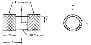
Fig.1. KDDP crystal with Cylindrical Ring Electrodes (CRE).

With such a configuration of electrodes, it is impossible to obtain a homogeneous electric field in the crystal [1] – [4]. That is a source of specific nonuniformity of transmission in the crystal cross-section. In order to obtain nonuniformity of the field distribution in the crystal <5%, the length of the crystal (2L) must be at least twice its diameter (2R). With such crystal dimensions, the width of the electrode W must be sufficiently large. For W / L = 0.65 – 0.7 it is possible to obtain field nonuniformity in the crystal dU = 3 – 4% when L / R = 2 or more ( Fig. 2 ).

Electric field distribution in KDDP crystals
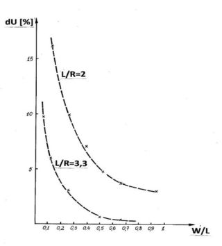
Fig.2. Nonuniformity of the electric field distribution (dU) for different geometries of KDDP crystal and width of CRE electrodes [1].

CRE KDDP Crystals
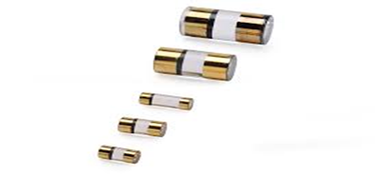
Fig.3. CRE KDDP crystals for Pockels cells with different apertures ( by INRAD Optics ).

The longitudinal electrooptic effect is a great advantage of KDDP crystal. Driving voltages U λ/2 are not dependent on the crystal dimensions and are the same for all Pockels cell apertures (Fig.3). This property can be very useful for various studies. This gives, for example, the possibility of constructing Pockels cells with large apertures at a very short crystal length.

Since the driving voltages cannot be reduced by the choice of crystal geometry ( like in the case of transverse electrooptic effect), it can be realized by increasing the number of crystals in the cell. In practice, double-crystal designs of longitudinal KDDP Pockels cells are offered for some applications. In these designs, KDDP crystals are mounted in series and supplied with opposite directions of electric field (Fig.4 b).

KDDP Crystals
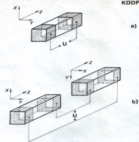
Fig.4. KDDP crystals of rectangular shape for Pockels cells with longitudinal electrooptic effect : a) for single crystal cell, b) for double-crystal cell.

KDDP (KD*P) crystals, that are grown from deuterated water solutions, are hygroscopic. Therefore, they require protection against atmospheric moisture. For this purpose, different technical solutions are used. KDDP crystals, generally are placed in appropriate hermetic housings.

In some technical solutions, crystals are mounted in housings closed by optical windows and filled with index-matching liquid to eliminate internal reflections. External surfaces of windows are antireflection (AR) coated. In other solutions KDDP crystals and optical windows are AR coated with reflectivity of < 0,25% per optical surface. KDDP crystals with high power Sol-Gel antireflection coatings are used.

All these solutions are widely used in flashlamp-pumped solid-state lasers as well as DPSS lasers.
Pockels cells using KDDP crystals can be also made in configuration with transverse electrooptic effect. This configuration is based on the r41 electrooptic coefficient and is realised as double-crystal design. Coefficient r41 is 3 times lower than r63, but the driving voltages can be reduced by selecting the crystal dimensions.

These constructions require using of both crystals with equal lengths of high accuracy. This is necessary to compensate for the natural birefringence. These configurations are also sensitive to temperature changes. Generally, transverse KDDP Pockels cells are mainly used as low-voltage modulators with small apertures.

Ryszard Wodnicki, PhD Eng.

References
[ 1 ] L.L. Steinmetz, T.W. Pouliot, B.C. Johnson, „Cylindrical, Ring-Electrode KD*P Electrooptic Modulator”, Applied Optics, Vol. 12, 7, pp. 1468-1471, (1973),
[ 2 ] Walter Koechner · Solid-State Laser Engineering, Springer Verlag .N.Y. , 1976.
[ 3 ] Z. Jankiewicz, E. Pelzner: „Modulator światła z wykorzystaniem wzdłużnego efektu elektrooptycznego Pockels’a” , Biuletyn WAT, vol. XXIX, Nr 1 (329), 1980, str. 21-32.
[ 4 ] R. S. Alnayli, Cs. Kuti, J.S. Bakos, I. Toth, „ Investigation of electric field distribution in Z-cut KDP Q-switch modulator crystals”. Quantum Electronics, 165(4), September 1989.

***