Optical Thin Film Deposition Technologies – Overview

Published: October 29, 2021

Optical coating technologies are key to modern optical systems allowing to produce mirrors, filters and other components with unique capabilities. For decades advances in this area have been driven by demand for more precision and functionality in laser, defense, medical and other high-performance applications. Today, using state-of-art fabrication technologies such as ion beam sputtering, evaporative deposition or advanced plasma sputtering, optical industry can produce thin film structures made of hundreds of layers at high speed and affordable cost. The article will review common fabrication methods and their applications.

Primer on Optical Coatings

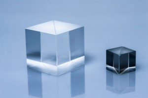
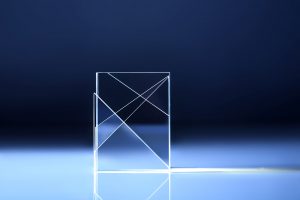
Optical coatings are one or multiple layers of material, usually dielectric and metal, deposited on the surface of optical material. The coating alters the way in which optical component transmits or reflects the light. It takes advantage of the way light is refracted or reflected as it passes through several layers with different indices of refraction. Depending on the type of effect created by the coating, they can perform variety of functions. The common application are anti-reflective coatings, which are used to reduce unwanted reflections from the optical surface (such as in everyday corrective glasses). On the other hand, reflective coatings are used to produce mirrors with high level of reflection. Polarization control, wavepass filters, optical beam splitters are other examples of applications in which thin films allowed significant size and cost reductions of many devices.

The state-of-art optical coatings provide high stability and can withstand wide range of temperatures, humidity and mechanical stress. The quality of optical coating is influenced by several factors. Starting with the design, performance depends on the structure and number of thin layers that make up the stack, their thickness, quality of materials and their refractive index. Since the first single-layer antireflection coating was introduced in 1930s, the industry has made a tremendous research and development effort that spurred new coating solutions and design tools. At the heart of these advancements are stable and repeatable optical thin film deposition technologies and processes.

Optical Thin Film Deposition Technologies

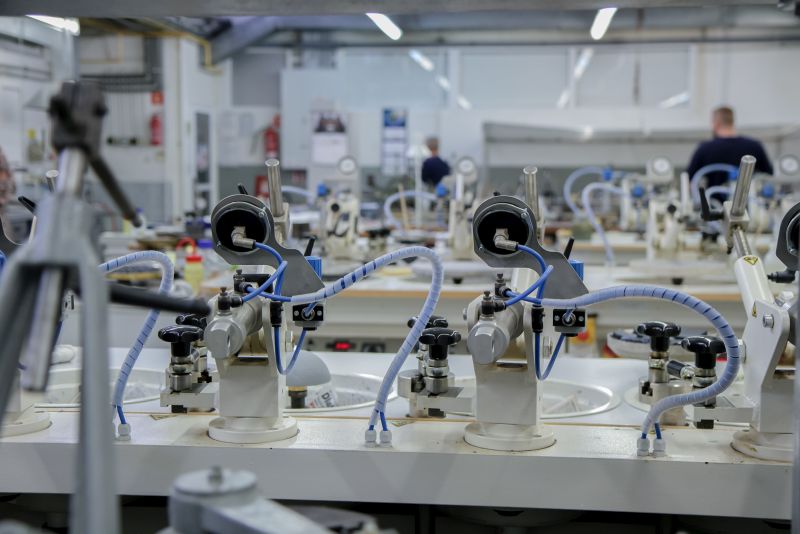
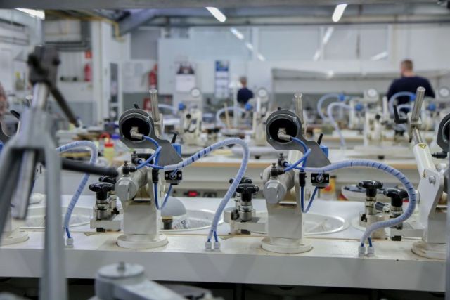
Optical coatings are produced using several deposition technologies. In principle there is always a target material (also known as source material, which is a portion of the material to be deposited on a product) and substrates, which are the optical elements that require thin film layers. The technologies applied differ between each other in terms of deposition technique, i.e. how the target material is transferred to substrates.

In this article we review the most typical, industry standard technologies with a proven quality, efficiency and productivity. We address the fundamentals, pros and cons as well as applications of E-Beam, Ion Beam Sputtering (IBS) and Advanced Plasma Sputtering (APS) technologies. Each provides a unique strength and weaknesses, in terms of capabilities and costs.

E-Beam Vapor Deposition

E-beam vapor deposition involves bombarding the source material with electron beam in a vacuum chamber to make it evaporate and deposit on the optical components, which are usually placed on the rotating planetary work-holders. In order to improve nucleation process and create more dense films, the optical substrate is heated to temperatures of up to 300OC. The resulting coatings are characterized by low strain and can be applied to wide range of component materials and geometries, including custom-shaped optics. However, they are of low density and porous. This makes them prone to an environmental shifting phenomenon, which means film’s refractive index can change when exposed to humidity. Ion-Assisted Electron-Beam (IAD E-Beam) additionally uses ion gun to bomb the substrate with a beam of highly accelerated ions to increase energies of the deposited atoms. Higher mobility of the molecules results in a denser film compared to standard e-beam technology, but also increases stress.

Apart from the film quality, the other downside of e-beam processes is low stability and errors. The evaporation process is challenging to control and as such can yield coatings with inconsistent performance. Thus, E-Beam PVD is a preferable deposition method for:

  • antireflective coatings,
  • less complex mirror,
  • complex geometries,

with low number of layers.
The advantage of the method is high flexibility, relatively low cost and high efficiency, as IAD E-Beam chambers allow for processing components in large batches. Thus, it is preferable technology for high-volume optics production, where productivity gains justify limitations in performance.

Ion Beam Sputtering Deposition

Ion Beam Sputtering is a stable and repeatable technology which uses ion beam to produce high-quality coatings in a highly accurate and predictable manner. It uses an ion gun to produce an extremely high-energy ion beam which bombards the source material and through the transfer of kinetic energy sputters particles from its surface. The energy of the sputtered particles makes it easily condense on the substrate forming a uniform and dense thin film layer. The technology produces dense and smooth coatings which are not affected by environmental factors and immune to temperature or humidity changes. Because the process involves a strict control and allows tuning of each material layer parameters, IBS allows for highly repeatable results and high yield across variety of coatings and substrate materials.

The downside of IBS is high cost of equipment and relatively high unit cost due to limited throughput and slow growth rates. This is the reason IBS is mostly deployed for applications that focus on high precision (including spectral precision), such as

Advanced Plasma Sputtering Deposition

Advanced Plasma Sputtering (APS) strikes a good balance between efficiency and performance, as the technology is fit for high-volume production while maintaining dense and accurate thin film deposition. As such, APS combines high throughput capabilities of evaporative deposition with quality comparable to that of IBS. APS uses hot cathode DC plasma source to produce a plasma that fills an entire chamber and sputters loose material ions from the target, which then deposit on the optical component. APS is well proven to produce complex structures, of more than 200 layers, without compromising precision, optical density or transmission features. Plasma Assisted Reactive Magnetron Sputtering (PARMS) is a version of APS which also uses plasma to sputter ions from source material, but in order to accelerate deposition rates, the plasma is guided to the target surface by a magnetic field produced by magnetron sources.
The cost and performance advantages of plasma-assisted technologies make it a preferable method for fabrication of:

  • precision filters, e.g. bandpass, notch and edge filters in wide wavelength spectrum as well as
  • polarization multilayers.

Especially in the military, medical or chemical markets, where optics need to adhere to strict quality standards, while the price still give an edge over competitors.

Optical Thin Film Deposition Technologies – Summary

Optical industry has many coating technologies to choose from and the choice is not always transparent. As discussed above, each option comes with its own advantages and limitations in terms of quality, price and production times. The right technology needs to be able to meet both performance specification of the optical system and its cost goals.

We recommend contacting Solaris Optics engineers if you are seeking to select a suitable optical thin film deposition technology.

Linear Variable Filters – Technology and User Perspective

Published: October 8, 2021

Linear variable filters are special types of filters where spectral response changes along the filter physical position. The main benefit of a LVF is that a single filter can provide characteristics of many filters or can simplify mechanical design when replacing diffraction gratings. More about types and applications of LVF we described in our previous publication Linear Variable Filters – Types and Applications.

The LVFs have been growing in popularity over the last decade, due to advancements in thin film deposition technologies. The focus of this article is to familiarize the reader with linear variable filters technology – design, manufacturing, as well as with advise from user perspective. Our goal is to provide basic understanding to design engineers who would like to benefit from the advantages of linear LVFs.

Technologies of Linear Variable Filters Manufacturing

LVFs can be designed based on various types of filters, including low-pass cut-off, high-pass cut-off or narrow band as well. Spectral response, as mentioned above, changes along one dimension, typically the filter length. Nevertheless, as mentioned by Mr Zdzislaw Choromanski, Head of Thin-Film Department in Solaris Optics:

“Variable filters can be also deigned and manufactured on a circular substrate, where the spectral response varies along the sample radius.”

Mr Zdzislaw Choromanski, Head of Thin-Film Department in Solaris Optics

The linear relation between the position and wavelength transmission, defined by filter slope (in nm/mm) is the most common design of a variable filter. It shall be remembered that those characteristics are not fully linear, but linear with certain tolerances. In a more general perspective the transmission versus position function can be custom profiled to achieve e.g. Gaussian profile.

When it comes to types of the deposited thin-films, variable filters are made of dielectric layers in a number that is sufficient to achieve performance. It may take tens but also hundreds, in some cases as many as 300 layers. The thin-films are coated typically on a flat sample of needed shape, e.g. rectangular, square or circular, dimensions of which shall allow to achieve the assumed wavelength range.

We asked Mr Choromanski, also about difficulties or limitations in LVF manufacturing:

“The main limitation in custom linear variable filters manufacturing is the spectral range the variable filter shall cover. Especially UV and low areas of the visible range are difficult because of dispersion of refractive index of the applied coating materials.”

Mr Zdzislaw Choromanski, Head of Thin-Film Department in Solaris Optics

LVFs are typically deposited with techniques that allow advanced control over the deposition process. Hence a conventional Physical Vapor Deposition does not allow to produce continuously variable filters. In most cases the deposition technology of choice is ion beam sputtering (IBS, also know as ion beam deposition). It enables extremely precise thickness control and deposition of very dense, high quality films. Also Electron Beam PVD with Ion of Plasma Aid enable manufacturing of linear variable filters.

Variable Filters – Key Outcomes

Linear Variable Filters are available both as stock, catalogue products as well as custom filters. Catalogue products cover the most common ranges, types and dimensions, as mentioned in the article. Nevertheless the variable filter technology provides a wide range of possibilities, including selection of specific sample shape, wavelength ranges, slope or custom position/wavelength characteristics. According to Mr Choromanski, when ordering linear variable filters it shall be remembered that the actual beam, which goes through the filter will be slightly blurred, which is a result of beam size and the varying spectral response, related to the beam position.

Linear Variable Filters in Solaris Optics

Solaris Optics is a manufacturer of custom variable filters (linear or other profiles) within UV to NIR range with maximum sample dimensions of 300 mm in diameter (for circular substrate) or 50-70mm length and 20-30 mm width for rectangular shapes.

Please do not hesitate to contact us if questions!
 

***

Basic crystals for Pockels Cells – KDDP, LiNbO3, BBO, RT

Published: September 24, 2021

Ryszard Wodnicki, PhD, Eng. 

Pockels cells for lasers in the visible and near-infrared spectral range

In most applications using laser sources, suitable modulation of the laser beam is necessary. The modulator is, therefore, an integral part of the laser system and it is used to control the main parameters of laser radiation as polarization, amplitude and phase.

From different methods applied for modulation of light, the most common is using Pockels effect in crystalline materials. This is the effect of changing the refractive indices of the optical material under the applied external electric field. The change of the refractive index is proportional to the value of the electric field, so the Pockels effect is also called the linear electro-optic effect.

The linear electro-optic effect occurs in crystals whose structure does not have a center of symmetry. Therefore, all these crystals, due to their non-centrosymmetric structure, exhibit piezoelectric properties. These properties require special designs and driving of pulse-controlled modulators, especially at high repetition rates.

Depending on the direction of the electric field with respect to the direction of the laser beam in the crystal, electro-optic modulators (Pockels cells) are divided into two types:

– with longitudinal electro-optic effect (electric field is parallel to the laser beam),

– with transverse electro-optic effect (electric field is orthogonal to the laser beam).

Most Common Crystals for VIS and NIR

Electrooptic properties of a large number of crystals have been investigated in the search for suitable materials for modulators. In the visible (VIS) and near-infrared (NIR) spectral range can be used following crystals:

KDP family KDP (KH2PO4)

ADP (NH4H2PO4)

KDDP (KD2PO4)

Lithium Niobate LiNbO3
Rubidium Titanyl Phosphate (RTP) (RbTiOPO4)
Potassium Titanyl Phosphate (KTP) (KTiOPO4)
Beta Barium Borate (BBO) (ß – BaB2O4)


From all these crystals only not numerous have found a wide application in practice. The most suitable and the most commonly used are KDDP and LiNbO3 crystals. Also, BBO is one of the good electro-optic crystals. Last time, BBO crystals are getting more and more attention and application in Pockels cells.

KDDP Crystals for Pockels Cells

KDDP (KD*P) crystals are grown from water solutions and are hygroscopic. They require special protection and construction of Pockels cells. But electrooptic properties of these crystals have caused great demand from laser technology. KDDP can withstand laser pulses with high power densities up to 1000 MW/cm2. They can be used over a wide range of wavelengths. Using these crystals, it is also possible to construct Pockels cells with both longitudinal and transverse electro-optic effects. This resulted in the rapid development of the technology of KDDP crystals, which now allows the production of high-quality optical elements with diameters of up to several hundred mm. This allows the construction of Pockels cells with very large apertures.

The possibility of using a longitudinal electrooptic effect is a great advantage of this crystal. In this case, the driving voltages are not dependent on the crystal dimensions and are the same for both 5mm and 50mm Pockels cell apertures. In addition, for solutions with uniform electric field distribution across the crystal (plasma electrodes [1], ITO), the length of the crystal can be very small in relation to the aperture. This is very important in laser systems with pulses of fs duration.

Basic parameters of KDDP and LiNbO3 crystals

Crystal KDDP LiNbO3
Crystal symmetry and class tetragonal 42m rhombohedral 3m
Density [g/cm3] 2,355 4,64
Hardness (Moh) 3 5
Solubility in water strong insoluble
Dielectric constants e1=58, e3=50 e1=96, e3=38
Transmission range [nm] 250–1900 350-5000
Index of refraction (633 nm) n0=1,504, ne=1,465 n0=2,296, ne=2,208
Electrooptic coefficients X 10-12 [m/V] r63T=26,4, r41T=8,8 r22T=6,6, r33T=32,2
Max. power density [MW/cm2] >1000 >300

T: unclamped

KDDP crystals exhibit low absorption in the near UV, visible and near IR. The piezoelectric properties of these crystals are relatively low.

So, they are commonly used in Pockels cells mainly as Q-switches. They are also used in Pockels cells for many other applications outside the laser resonator as fast optical shutters. KDDP Pockels cells are used for the selection of nanosecond laser pulse from Q-switched pulses and selection of single ps or fs puls from the train of laser pulses.

LiNbO3 Crystals for Pockels Cells

LiNbO3 crystals are grown by the Czochralski method and are not hygroscopic. They are excellent electro-optic materials. Lithium niobate has a broad transmission range, from the visible up to medium infrared. Due to the high value of the refractive index (n>2), these crystals require appropriate anti-reflection coatings.

The electro-optic properties of LiNbO3 (class 3m) show, that the longitudinal electro-optic effect cannot be realized in these crystals. The only transverse electro-optic effect is possible, which allows the construction of modulators (Pockels cells) with low driving voltages.

LiNbO3 crystals can withstand laser pulses with power densities up to 300 MW/cm2 for 10 ns pulses and are very often used as Q-switches. In CW applications they can be used at average powers of laser beam up to 100 W/cm2.

Lithium niobate has a large piezoelectric constant. Strong piezoelectric properties can disrupt sometimes Q-switching and modulation. The piezoelectric ringing phenomenon is a result of rapid high voltage changes and causes modulation of the contrast ratio. This requires the use of appropriate methods for the dumping of the ringing effect.

Properties of beta-BBO crystals

Crystal beta-BBO
Crystal symmetry and class trigonal, 3m
Density [g/cm3] 3,85
Hardness (Moh) 4,5
Solubility in water very low
Transmission range [nm] 200-2600
Index of refraction (1064 nm) no=1,6551, ne=1,5425
Electrooptic coefficients X 10-12 [m/V] r22T=2,7, r22S=2,1
Max. power density [MW/cm2], 1064 nm, 10 ns 4500

T: unclamped

S: clamped

BBO and RTP Crystals for Pockels Cells

BBO (β-barium borate) is a non-centrosymmetric, negative electrooptic crystal. As a result of its high damage threshold, excellent transmission in the range from UV up to NIR, BBO has become interesting material for Pockels cells. BBO, like LiNbO3 crystals, can be used for modulation in a configuration with a transverse electro-optic effect. The piezoelectric properties of BBO are much lower than KDDP. Low piezoelectric ringing makes BBO crystals attractive and suitable for Q-switches in diode-pumped and lamp-pumped solid-state lasers. They are suitable also for laser pulse picker devices and for coupling laser beams within and outside regenerative amplifiers.

In applications, where the piezoelectric ringing phenomenon is a big problem, the RTP crystal can be used in the Pockels cell. RTP belongs to the KTP crystal family and is promising electrooptic material. RTP exhibits an extremely low piezoelectric effect, large electro-optic coefficients and transmission in the range of 350 nm up to 4000 nm. Currently, it is the only crystal material with a ring-free operation. In addition, is non-hygroscopic material with a Mohs hardness of 5. RTP Pockels cells are constructed as a two-element design for temperature compensating.

Summary: Selection of Crystals

The selection of the appropriate Pockels cell for Q-switch operation or operation outside the laser resonator depends on many parameters and conditions. It is determined by excitation of the active medium, type of laser operation, laser pulse parameters, required repetition rate, switching speed and driving voltage of Pockels cell, as well as wavelength and polarization degree.

Presented data and properties of electrooptic crystals should be helpful for Pockels cell users. We are also happy to advise for proper crystal selection for specific Pockels cells applications.


[1] J. Goldhar and M. A. Henesian, Electro-optical switches with plasma electrodes, Opt. Lett. 9 (3), 1984.

Linear Variable Filters – Types and Applications

Published: August 31, 2021

Linear variable filters (LVF), also known as continuously variable filters, or gradient filters, are special types of filters, where the filters’ spectral response changes continuously (or quasi-linearly), in a defined manner, along one dimension. In an example case a change of a linear variable filter position by 4mm will shift the filter center wavelength transmissivity e.g. from 500 to 520 nm, so by 20 nm (a slope of 5 nm on each 1 mm). The gradient may vary and is selected for a particular application.

In practice, LVFs enable to replace setups with multiple filters with a single filter, simplifying design and reducing costs of many measurement devices.

By design, LVFs are dielectric filters working on interferometric principles. They are manufactured by covering a filter substrate (for instance fused silica) with many thin film coating layers. The thicknesses of the thin film layers change along one filter direction (typically the length of the filter), creating the varying spectral response. Solaris Optics manufactures custom linear variable filters in its premises in Poland and in the below article we discuss the basics, types and main application fields of linear variable filters.

Conventional Wavelength Separation Techniques

A typical example of wavelength separation application is spectroscopy. In spectroscopy, wavelengths have been conventionally separated by diffraction gratings, prisms or a set of filters.
Diffraction gratings, for instance, have certain advantages for uses where light intensity is relevant, however as they are elements based on angle-based dispersion, they require more space and more complicated mechanical designs to work. Compared to diffraction gratings, linear variable filters require less space, yet allow smaller devices to be designed.
Another wavelength separation alternative – a set of filters, makes it necessary to ensure filter change mechanism, which can be realized e.g. by locating filters on a rotating wheel. This requires space, limits the possible pass bandwidths and rises overall cost.
In case of LVF the filter is held in a device so that a relative movement between the filter and the signal source is feasible. By moving the filter (or signal source) along the gradient axis, specific wavelengths are transmitted or blocked, according to the filter characteristics.

Main Characteristics of Continuously Variable Filters

LVFs are offered within UV to mid-IR range, e.g. from 230nm (then a filter range of e.g. 230-500nm) up to 5um (filter range 2.5-5 um). Apart from filter spectral range, they are typically characterized by bandwidth or cut-off wavelength, slope (change of center wavelength in nanometers per millimeter), pass bandwidth (usually specified as full width half maximum FWHM), transmission levels, filter blocking and physical dimensions. A manufacturer shall prepare also a chart showing the actual transmission wavelength versus filter physical position. In practice this chart shows actually a quasi linear relation between the transmissivity and position.

Some example specifications of commercially available continuously variable filters include:

  • a slope of e.g. 5nm/mm, 20nm/mm, or any, e.g. 90nm/mm,
  • pass bandwidth of less than 1% up to roughly 2.5% of the center wavelength,
  • transmission of 50% to 90%,
  • filter blocking of about OD3-4,

whereas a good level of linearity would be e.g. +- 1%.
The actual characteristics is largely affected and limited by the filter wavelength range, which for bandpass filters may be e.g. 230-500nm, 300-750nm, 700-1100nm, 1.3-2.6 or 2.5-5um. It is up to a specific application to design or select a suitable filter type.

Types of Linear Variable Filters

Linear Variable Filters can be created with various defined spectral properties, where the ratio between transmissivity and position may be also highly non-linear. However due to design convenience and requirements in many applications a linear characteristics is advantageous and in practice is the most sought. Variable filters are typically offered as long pass (Long Pass Variable Filters), short pass (Short Pass Variable Filters) and bandpass (Bandpass Variable Filters).

An interesting set of features can be achieved by using both Long Pass Variable Filters and Short Pass Variable Filters, so that they can be independently moved along the same axis. In such a setup it is possible to achieve a Linear Variable Bandpass Filter, which central wavelength (transmission spectrum) and bandwidth can be tuned continuously and adjusted as needed.

Applications of Linear Variable Filters

Continuously variable filters are applicable in the domain of measurement and detection. Hence they are used in many spectroscopic and analytical applications, in either laboratory as well as process applications. Uses such as gas analysis, material identification, wavelength sensors, hyperspectral imaging are some examples, where LVF are advantageous.

LVFs enable also more advanced designs. For instance when combined with detectors, such as line or square CCD/CMOS sensors the filters allow to build a compact and rugged detectors with large aperture and high transmission, which yields short measurement time, high suppression of straight light excellent signal to noise ratio.

As described above, linear variable filters offer a number of advantages compared to conventional wavelength separation techniques. Solaris Optics, as a throughout manufacturer of linear variable filters offers its customers support in filter design and selection. Please feel free to contact us!

***

Pockels cells – design, manufacturing, selection – interview

Published: July 30, 2021

Interview with Mr Ryszard Wodnicki, PhD, Eng.

Mr Ryszard Wodnicki, PhD Eng, is a co-founder of Solaris Optics and a scientist responsible for the development of Pockles cells technology in the company. In todays’ interview we discuss about Pockels cells technology, applications, design, manufacturing and selection. We aim to provide necessary information and explanations to design engineers who seek Pockels cells for their projects.

Dear Dr Wodnicki, let’s start from the basics – what is a Pockels cell?

Pockels cell is a device, an optical subsystem, which modulates light. It utilizes an electrooptical effect (so-called Pockels effect), which is a change of refraction indices of the optical material when an electric field is applied. This effect, named after the discoverer, appears only in crystal materials, typically anisotropic crystal (i.e. having different refraction indices in different directions). Refraction indices of such anisotropic crystals are typically described in a form of an ellipsoid called indicatrix.

When an electric field is applied in such crystals, the refractive indices change (the ellipsoid gets deformed). Depending on the direction of the electric field in the crystal, as well as on the direction of light propagation, induced birefringence is obtained.

A Pockels cell uses birefringent crystals (having two values of refractive index) and such configuration of the light and the electric field in the crystal, so that the best effect of modulation is achieved.

Pockels effect is a linear effect, which means the refractive indices change proportionally to the value of the applied electric field. By comparison, another known electro-optic effect – the Kerr effect is non-linear so that the refractive index values changes are proportional to square values of the electric field. Hence it is not commonly applied – not only requires high voltages but also takes place in liquids, but also due to other assisting phenomena.

What are the main types of Pockels cells nowadays?

There are two main types:

  1. A cell with a longitudinal electrooptic effect – where the electric field and the light beam have the same direction and are parallel to the direction of an optical axis of the crystal. A relevant feature of this configuration is, that the driving voltages are independent of the crystal dimensions. For instance, a Pockels cell with an aperture of 5mm has the same control voltage as a cell with an aperture of 50 mm.
  2. A cell with a transverse electro-optic effect. In this configuration, the direction of the electric field is perpendicular to the direction of the light beam. A relevant feature of this configuration is the possibility of a significant reduction of driving voltages.

What about applying a voltage to the beam input/output surface in the case of longitudinal effect? Isn’t it challenging?

Yes, it is. To have high transmission of the cell, the electrodes are manufactured as rings on the side surface. If a crystal is of cylinder shape, along which travels the light beam, then the electrodes are made as rings localized on the lateral surface at both ends of the cylinder. It is a so-called Cylindrical Ring Electrode (CRE) configuration. But, such a setup, by definition does not give a homogenous field, because the electrodes are not made directly on the optical surfaces of the crystal. Therefore the crystals shall have appropriate lengths so that a maximum of field uniformity can be achieved. In Solaris Optics we achieve about 97% of uniformity of the field in such standard configurations.

So, given the fact that in longitudinal Pockels cells the electric field is inhomogeneous, why actually use them? Why not use only transversal Pockels cells?

The most common application of Pockels cells is the switching of losses in laser resonators (Q-switch) in order to generate short, high power laser pulses. In these applications, the uniformity of the electric field distribution in the crystal doesn’t have to be high. Uniformity of 95% is quite sufficient even for lasers with a high gain of laser medium.

Crystals of the KDP-group (especially KDDP) were developed quite early. They are grown from water solutions. Unfortunately, they are hygroscopic (attract water from surrounding environments) and require protection against atmospheric moisture. Nevertheless, this technology was developed tens of years ago. Nowadays it allows obtaining homogeneous optical elements from KDP and KDDP crystals with dimensions up to several hundred mm.
For application as Q-switches, Pockels cells with apertures of up to about 15 mm are needed. Using KDDP crystals with CRE electrode configuration, Pockels cells can be not as expensive as others with transverse effect.

What is the relevance of crystal size?

From a grown crystal a homogenous piece must be selected, then a monocrystal can be cut for a Pockels cell.
In addition to Pockels cells with apertures down to 15 – 20 mm, a wide range of applications require cells with bigger apertures such as 50 mm and more. This is where KDP and KDDP crystals are used.

In the case of other crystals, such as Lithium niobate (LiNbO3), where only transversal electrooptic effect occurs, the driving voltage depends on the crystal width to length ratio. This allows for a significant reduction of the Pockels cell driving voltages.

Such crystals are grown in more challenging conditions, and generally, the growth is more complicated. Hence only relatively small dimensions of crystals can be manufactured. To produce a LiNbO3 Pockels cell with an aperture of 20-30 mm, we are already on the limit of technological capabilities. So, when a small aperture is needed, then a transversal Pockels cell from lithium niobate, lithium tantalate (LiTaO3), or recently also barium borate (BBO) can be used. Those are offered in apertures of 5-6 mm and their prices are high compared to e.g. KDDP Pockels cells.

Why do we actually need a larger aperture?

An aperture is a cross-section dimension, where enters the beam. If the beam diameter is of few mm, then a 5 mm aperture of a crystal is sufficient. However, for a beam of 10 mm in diameter, the aperture shall be about 12-15 mm – this depends on specific application.

Do Solaris Optics clients already know what Pockels cell they need or are they asking an advice?

There are both types. Some clients require advisory. In Solaris Optics we developed designs for KDDP and lithium niobate and within those crystals, we can move. For visible (VIS) and near-infrared (NIR) spectrum KDDP Pockels cells are quite convenient, as there are no limits towards aperture size. They are commonly used as Q-Switches. In many applications, there are also niobate crystals applied with a transversal effect and low control voltage, but they have other disadvantages, such as lower resistance to laser beam power or, as small crystal (aperture) dimensions.

Dr Wodnicki, you are talking much about the control voltage – why shall a designer seek a lower control voltage?

Well, this is not a goal by itself, but e.g. in the case of KDDP, we are talking about kilovolts, so high by definition. However, when it comes to niobate crystals, it is possible to steer those with a lower voltage. But when a high frequency is necessary at a higher voltage, it requires a more complicated control setup (e.g. to achieve the required voltage amplitudes at high frequencies). If voltage is few times lower then the driver size is few times smaller. This gets very relevant in e.g. medical, industrial or defense applications.

Regarding applications – what are the most typical applications of Pockels cells?

We can group typical applications into few categories:

  1. Q-switch – modulator of lasers’ resonator goodness – it is used to generate gigantic pulses, i.e. short, high-power laser pulses. Q-switches are applied in lasers that require such short and high power pulses. So typically those will not be used in measurement (with some exemptions) or welding applications. The role of a Q-switch is to collect energy in the active material. This energy is then released as a single pulse in a short time. This is advantageous e.g. in ophthalmology procedures (e.g. coagulation), defense (e.g. range finders), LIDAR (e.g. air pollution measurements), industry. One of our clients used Pockels cells for dermatology (e.g. tattoo removal and skin therapies), where there’s a need to evaporate something from the skin.
    Q-switch allows to generate 10 – few tens nanosecond pulses. It is perhaps the most common application of Pockels cells.
  2. Due to fast operation of the cells (are able to quickly change light polarization) they are used for 2 further applications:
    • to separate one pulse from a row of pulses – where a laser generates a sequence of pulses and 1 of the pulses must be separated – so called pulse picking
    • pulse shortening – where a part of a longer pulse must be cut out; this finds applications e.g. in obtaining femtosecond pulses in both practical (e.g. medical) and research domains.

    In the above cases Pockels cells are used outside the laser resonator.

  3. Scientific and research applications – the cells can be used inside and outside the resonator; they are needed for solving scientific issues, e.g. as a setup for amplitude modulation.
  4. Regenerative amplifiers for femtosecond lasers – since femtosecond lasers appeared on the market there has been an issue to strengthen those fs pulses. The pulses, of very low energies, are injected into an active material, where they ger amplified. Pockels cells are used on the input and output of the medium.

What are the most relevant specifications of a Pockels cell from a perspective of a design engineer?

A client ordering a Pockels cell shall explain to us the optical specifications:

  • wavelength of the laser radiation (which helps to select the cells’ crystal),
  • beam diameter (which allows selecting aperture),
  • working conditions (what working frequency for the cell, laser beam power and damage threshold (pulsed or continuous laser),
  • required transmission of the Pockels cell, because crystals have different refraction indices and require suitable AR coatings; if clients seek transmissivity of 98%, then we need to plan AR thin film coatings accordingly, to achieve the requirements.
  • type of crystal – typically clients suggest a specific crystal, however if needed, we also advise,
  • wavefront deformation – for Pockels cells typically lambda/4 and lambda/8 are used; if higher requirements (smaller deformation) are necessary, then additional crystal processing is needed.

So, how shall a design engineer start to select good Pockels cells, what to remember of?

Well, the first thing to think of is the cell aperture and type of crystal. Type of crystal is defined by wavelength, transmissivity and damage threshold, for instance, niobate crystals are characterized by lower damage thresholds, whereas KDDP higher, so are applied for higher power lasers.

Also, systems’ working conditions are relevant, e.g. is it for a Q-switch or amplitude modulation. Based on such information a Pockels cell type can be selected.

What sort of Pockels cells are manufactured by Solaris Optics?

In Solaris Optics we developed and manufacture Pockels cells with the following crystals:

What are the main applications of KDDP and lithium niobate-based Pockels cells?

There are many applications, as mentioned above. The main is Q-switch and modulation outside the laser resonator, pulse shaping and pulse picking. It is used in industry, healthcare, military, research and development.

What is the most critical when manufacturing Pockels cells?

Attention shall be put mainly to the crystal. Apart from crystal, there are mechanical and electrical issues with housing – it must be precise. The electrodes are golden Au coatings deposited directly onto the crystal – the connections must be reliable and harmless.

In the case of KDDP, also crystal protection against atmospheric moisture.

Regarding crystal, the orientation of the optical axis, as well as the processing of the input/output surfaces, must be accurate. In specifications, the parallelism of the surfaces is typically 20 arcsecs. It is relevant, because it may cause beam deflections and wavefront deformation.

So, it is the parallelism of input/output surfaces, wavefront deformation, accuracy of optical axis orientation, AR coatings.

What about reliability of Pockels cells, what issues may appear during operations?

A Pockels cell is selected for a specific laser and its application. A number of criteria are taken into account, such as required pulse parameters, repetition rate, driving voltage, contrast ratio, switching speed, damage threshold and others. An important parameter is the intensity distribution in the laser beam cross section. The threshold of the cell damage by a laser beam is determined for the beam with homogeneous or Gaussian intensity distribution.

A number of devices using solid-state lasers use a multimode beam. The intensity distribution in the cross-section of such a laser beam contains a lot of spikes with peak power densities well above the average value. This is a source of damage of the crystal (and windows with AR coatings) by causing multiple autocollimation trains inside the material. In such lasers, the permissible power of the laser pulse should be selected very carefully.

How long can Pockels cells work effectively?

By using Pockels cells in accordance with the specifications, and taking care of the quality of the transmitted laser beam, they can work for many years.

In the case of KDDP crystals, which are hygroscopic, it is important to protect the crystal against the influence of atmospheric moisture. This technology can extend the life time of the cell and is an important issue for designers.

For that reason KDDP Pockels cell should not operate with a constant applied voltage. Such a type of operation is specifically not recommended and significantly shortens the lifetime of the cell.

Ultimate lifetime of the cell is eventually determined by the damage of crystal and protective windows.

Dr Wodnicki, thank you for the interesting talk!

***

Subsurface Damages Reduction for Precise Optics Manufacturing

Published: June 29, 2021

Solaris Optics is a custom optics manufacturer with a focus on precision optics. Precision typically comes out as a result of all manufacturing steps and is described by final specifications including dimensions, form error, surface quality, radius, etc. as well as via actual, measured performance of optical elements.
In order to further develop its capabilities in precision optics manufacturing Solaris Optics regularly investigates its potential improvement areas. One such domain, addressed by Solaris Optics with support of EU funds, is the occurrence of so-called subsurface damages in glass optical elements.

Subsurface damages as a source of optics quality deterioration

Subsurface damages are defects, such as cracks, but also contaminants or residual stresses, that appear below the optical surface. Subsurface damages caused by element manufacturing appear typically from 100 nm to 5 um below the components surface.
Such damages in final glass optical elements affect the component performance. For instance when an element is used with a high power laser the laser energy is absorbed by the optics, especially in damage areas, which leads to component faster deterioration and damage. Similarly, in measurement systems, optics subsurface damages cause additional scattering and can reduce the signal to noise ratios.
The subsurface damages cannot be fully avoided, regardless of manufacturing techniques applied, nevertheless they are a common problem, which requires to be addressed.

Sources of sub-surface damages in optics

A crucial question to manufacturers is how to reduce the occurrence of subsurface damages in the manufacturing steps and in the final parts. Reduction of the damages would significantly speed up the manufacturing process and improve the product quality.
To give a manufacturing process perspective – a simplified glass optics manufacturing process can be described as below:

  1. Cutting elements from a glass block
  2. Machining the elements
  3. Grinding
  4. Polishing the elements + optional polishing via MRF (for ultimate precision)
  5. Cleaning the elements
  6. Measurements and thin film deposition


Fig. 1. Polishing technologies – subsurface damages

The problem of subsurface damages, especially cracks, was identified to appear during the grinding processes. It is proved experimentally and described in literature.
Grinding is a process of material removal, towards the expected component shape and dimensions. It is an iterative process, where each iteration removes a material layer along with the deepest damages. Each grinding step creates further, but smaller damages, so that in each step a smaller amount of material and smaller damages are removed. In result, after several steps the surface and subsurface damages are small enough so that the element can go to final polishing.
When a part goes to polishing process it is, as mentioned above, not free from subsurface damages. Hence polishing shall finally reduce the subsurface damages existing after the grinding process. With such demands polishing becomes a time consuming process, significantly affecting the overall production time.
Hence it can be assumed that reducing the occurrence of subsurface damages before the components go to polishing (hence on the grinding phase) shall considerably reduce manufacturing times and costs.

Reduction of subsurface damage via diamond grinding

In order to address the issue Solaris Optics started an R&D project, which aims to describe the development of subsurface damages during the production steps and to propose alternative manufacturing techniques, that would allow to mitigate the issue of subsurface damage.
Based on literature and research in available technologies Solaris Optics engineers identified grinding with diamond palettes as a potential technique to improve grinding precision and reduce the sub-surface damages caused during this phase.
In order to apply the diamond pallets Solaris Optics needed additional grinding capabilities and purchased a single-sided CNC grinding machines from Dopa Diamond Tools.

“The implementation of this technology at Solaris Optics is aimed at eliminating the formation of subsurface damage resulting from traditional cutting and grinding processes. As a result, the quality of the offered products will improve, the grinding and polishing time will be shortened, which in turn will translate into shorter delivery times for our customers.”

Kamil Łęcki, Technical and Investment Manager at Solaris Optics

The measurements of results, i.e. the actual subsurface damages at different stages of manufacturing, will be measured via microscopic techniques, after gently removing the surface layer with MRF polishing machine (in raster mode) and chemical etching.

Expected results

The investigation shall allow Solaris Optics to improve the optics manufacturing process for planar optics, such as mirrors, windows, blanks, prisms, etc. The main benefits for clients include shorter lead times and lower costs with improved final product quality (i.e. less scatter, better durability).
Solaris Optics observed positive results of the initial tests and becomes optimistic towards the project goals.

*

The R&D investigation and investment is a part of a project titled “Development of R&D infrastructure of Solaris Optics S.A. as a way to implement innovation” co-financed by the European Regional Development Fund under the Regional Operational Program of the Mazowieckie Voivodeship for 2014-2020, Sub-measure 1.2. Research and development activities of enterprises.

***

Optical Polishing Technologies – Review

Published: May 30, 2021

Optical polishing is one of key production steps when it comes to performance and quality goals of today’s optics. In this article we discuss the most common polishing techniques for high-precision optics.

Optical polishing is a finishing process that is crucial to meet the flatness, thickness, or finish specifications of high-precision optical systems. Luckily, advancements in this area allowed to constantly push the envelope in terms of possible surface smoothness and accuracy to obtain. While almost all polishing methods involve the removal of a certain amount of material from the surface, there is rarely one size fits all. Depending on materials, sizes, geometries and surface finish requirements, engineers need to choose an optimal approach to achieve the desired effect. Each available technique uses a unique method to remove the layer of material and has its own strengths and weaknesses.

Pitch Laps and Polishings Pads – Traditional Techniques

Pitch polishing is a traditional technique for finishing optical surfaces known for its precision and accuracy. The method uses polishing pitches stroked over the optical surface to obtain a high level of flatness, low surface roughness, and cosmetic quality with minimal surface defects. Pitch is obtained through the distillation of tar from wood or petroleum and is formed to fit the optical surface to be polished. Thanks to its softness it does not scratch the surface but when used with polishing abrasive, it reduces the surface roughness and provides exceptional quality. There are many fine polishing compound types available on the market, including cerium oxide, alumina, colloidal silica, and many proprietary solutions from multiple vendors.


Fig. 1. Optical polishing facilities – Solaris Optics

Pitch polishing is regarded as an ultra-precise method that offers high quality and flexibility in terms of fabricated components, including lenses, optical flats, prisms, or filters in a wide range of geometries and sizes. However, low efficiency and the need for strict manual control and maintenance have limited its use to low-volume, custom parts where the emphasis is on accuracy and performance, not efficiency and output. This has led to increased interest in the use of synthetic polishing pads which strike a good balance between performance and productivity. This high-speed polishing method uses pads made of foam material, such as polyurethane, which is pressured against the optical surface to perform material removal. The polishing is a combination of mechanical and chemical processes, which means engineers are to determine the optimal pad type and polishing compound for their applications. The pads can operate at much higher speed and pressure compared to pitch laps, which led to an exceptional output increase.

In contrast to pitch laps, pads don’t conform to the shape of the finished component and thus require a surface which is already fabricated to high precision. The range of possible uses is narrower, but still, pads are proven to meet surface finish and figure specifications for even demanding applications. Thanks to its cost- and time-effectiveness it has become a standard technology for high-volume finishing of e.g. ophthalmic lenses, precision optics, mirrors, and other optical components made of a variety of materials.

Continuous polishing is a technique designed fpr finishing flat surfaces, a task that is difficult with conventional methods. The fabricated part is placed on an annular pitch lap which is several times larger and rotates continuously. To achieve uniform wear, the part is held by holders in a way that allows for synchronous rotation with the lap. To ensure the flatness of the lap, a large flat conditioner is used. For parts with two parallel faces, it is possible to use twin polishers with a lap on top and bottom of the part polishing both surfaces simultaneously. Continuous polishing is capable of producing high-quality, smooth flat surfaces in sizes of up to one meter in diameter.

Learn more about Solaris Optics traditional polishing services.

The traditional approach meets expectation of many todays applications. Nevertheless, the evolving shapes of optical surfaces as well as the ever increasing surface quality requirements have been pushing egnineers towards development of new, more advanced polishing methods.

New Mechanical Polishing Processes

Several novel techniques have been developed capable of fabrication of aspheric and freeform optics with a high level of accuracy.

Bonnet polishing is a sub-aperture method that uses a spinning inflated rubber membrane in a spherical form covered in polyurethane or other polishing material. The bonnet is inflated by air pressure and when pressed against the surface conforms to the aspheric or freeform geometry. Removal rate depends on the type of tool and abrasive slurry used and is a function of dwell time, speed and pressure.

Optical polishing MRF
Fig. 2. Optical polishing MRF – Solaris Optics

Another example of a mechanical method is fluid jet polishing based on a stream of abrasive slurry projected at high pressure at the piece through a nozzle. The impact of the abrasive particles in the slurry removes material from the surface at a rate dependent on medium characteristics and working pressure.

The ion beam figuring method uses an ion gun to bombard the optical surface with the ions and thus removes the material in a highly controlled and predictable way. The contactless technology is well established to polish custom optics in diameter of up to thousands of millimeters with high-precision, low errors, and no sub-surface or edge defects. Heavily accelerated ions reach the surface with considerable kinetic energy causing atom sputtering from the target surface. The method produces high-end surface quality with nano-precision, but requires vacuum conditions and has a relatively low material removal rate. Hence, it’s usually used as a corrective polishing method after the piece was pitch polished. The high cost and processing times have prevented this method from being used in volume production.

Another contactless technique is a high-intense laser beam, usually from CO2 source, which can be used for melting and ablating a thin surface layer of optical material to reduce roughness and improve figure quality. Melting of the material leads to smoothening of the surface thanks to surface tension in the softened layer. No material removal takes place as the surface subsequently solidifies. The method offers a promise of high-precision finishing of freeform optics, does not generate any waste and recent advancements have considerably shortened processing times. However, the cost of laser polishing equipment remains a consideration.

For more information regarding Solaris Optics MRF corrective polishing – please do not hesitate to contact us!

Magnetorheological finishing (MRF) is a relatively new but already well-established technology that allows the fabrication of mild aspherical optics, or high level polishing of surfaces, which meet even the strictest specification. MRF finished optics can achieve exceptional form accuracy with figure error as low as ~1 nm RMS, mid-spatial frequency errors of ~1 mm, and surface roughness of ~1 Å RMS. The method involves magnetorheological fluids which contain magnetizable particles and form a polishing layer over a rotating wheel with a magnet under the surface. As the wheel rotates, the polishing agent is pressed against the worked surface and material removal is performed in a deterministic manner. Although being a sub-aperture technique, MRF has proven to be an efficient and precise method for the fabrication of optical pieces across a wide range of geometries and sizes. A prime example is five 204mm mirrors fabricated by Solaris Optics S.A. for Paranal Observatory using MFR, stress mirror polishing, and SSI metrology. The use of MRF allowed to achieve 22.4 nm PVr and <λ/20 PV across the full aperture.

Summary

In the above article we reviewed the main mechanical polishing technologies, as used in industry. As mentioned it is always up to an engineer to select one of those. Solaris Optics engineering & production team will be happy to answer your questions regarding your polishing needs!


***

Optical Modulators for Laser Q-switching

Published: April 28, 2021

Optical modulators are key building blocks for many optical systems and functions, including data transmission, laser printing, Q-switching, active-mode locking, shifting beam spectral frequency and much more. In this article we will discuss the two major modulator types for laser Q-switching: electro-optic or acousto-optic modulators. While both allow for producing high-power, ultra-short laser pulses, system designers should know the strong and weak points of each technology to choose the best option for their application.

The basics of Q-switching

Q-switching is a common technique to produce ultra-short laser pulses. It involves increasing resonator loss with the use of a modulator, which leads to increase of accumulated electron population difference in the lasing medium as the pump is continuously delivering power. When the modulator is set to ‘open’ mode, the resonator quality factor Q rapidly increases which results in a high-intense, ultra-short laser pulse. Not every laser can be Q-switched and the technique is mostly used with Nd:YAG and other solid state lasers, while gas lasers usually depend on other solutions.

Optical modulators - Pockels cells
Fig. 1. Optical modulators – Pockels cells

While it is possible to build Q-switches based on mechanical or dye modulators, the acousto-optic and electro-optic options provide the best performance in terms of possible on/off frequencies and resulting output power. The ease of transforming signal from electrical to optical form is another factor which contributes to popularity of these devices.

Acousto-optic modulators

Acousto-optic modulators take advantage of the phenomena in which an acoustic wave propagating in an optical medium produces a periodic modulation of the optical medium refractive index. The resulting phase grating leads to diffraction of incident light and the effect is used for spatial, temporal, and spectral light modulation. The structure of acousto-optic modulator consists of a block of optical material, such as Quartz, fused silica, flint glass or tellurium dioxide, with an attached piezoelectric transducer to its side. A radio-frequency driver generates acoustic signal which scatters passing beam in a predictable manner. The amount of light scattered is dependent on the amplitude of the piezo-induced sound wave within the optical material.

The ongoing technological advancements in terms of materials and broadband transducers have made acousto-optic modulators a reliable technology for laser beam control. The traditional application is in high-power Nd:YAG systems in industrial and military applications.

While acousto-optic modulators offer low insertion loss, they generally provide lower gain compared to electro-optic modulators. The frequency of operation ranges from 27 MHz to 1 GHz, which means they are less fit for high bandwidth applications. However, acousto-optic devices usually have an advantage of not requiring high driving voltage and are well suited for broader wavelength spectrum in IR, VIS & UV range.

Electro-optic Modulators

Electro-optic modulators (EOM) are more flexible option in terms of light parameters they can modulate – they allow to control the amplitude, polarization or position of an optical beam. Electro-optic modulators provide a backbone to modern communication technologies, analog and digital processing, optical sensing and many more. What makes electro-optical modulators stand out from its acousto-optic or mechanical counterparts is much higher frequencies, in GHz range. This makes it a preferable solution for high-speed optical communication as it allows for data-transfer rates that are not matched by other modulation techniques. EOM-based Q-switching solutions offer high speed and high gain, although usually higher voltage is required compared to acousto-optic modulators. Hence the most common use is in the visible spectrum (as the half-voltage increases with wavelength). However Pockels cells for infrared (up to far IR) are also available on the market.

The electro-optic phenomena describes the change in materials’ anisotropic optical properties under the external electric field. There are several technologies that make use of an electro-optic effect to modulate the light wave. The common principle is the ability to modulate optical properties of a material, e.g. index of refraction or natural birefringence, in a controlled manner by applying an external voltage.

Pockels Cells Optical Modulators
The linear electro-optic effect, known as Pockels effect, can be observed in crystals lacking a center of symmetry where birefringence is produced in a material proportionally to the applied electric field. The most common materials for Pockels cells are electro-optic crystals such as di-deuterium phosphate (KDDP), barium borate (BBO), lithium niobate (LiNbO3), lithium tantalate (LiTaO3), and ammonium dihydrogen phosphate (NH4H2PO4, ADP). Another alternative for a Pockels cell crystal is rubidium titanyl phosphate (RbTiOPO, RTP), giving an RTP Pockels cell, oftentimes used in neodynium lasers, such as Nd:YAG.
Pockels cells in combination with polarizers can be used as amplitude and phase modulators with the advantages of low drive voltages, low insertion loss and ability to handle high optical powers. The device is capable of reaching modulation frequencies of gigahertz range and can serve as shutter with response time of less than 1 nanosecond.

A sole Pockels cell itself can serve as a phase modulator, as it has a capability to change phase of the passing light when it travels in a direction of one of its optical axes without affecting its polarization. A common setup for light intensity modulation is a Pockels cell placed between two polarizers perpendicular to each other. At zero voltage the crystal does not change light polarization, causing the beam to be fully blocked by the second polarizer. Applying voltage induces a birefringence in the crystal, which in turn changes light polarization from linear to elliptical and the light can pass through the second polarizer. The amount of light passing depends on applied voltage, and specifically at the half-wave voltage the modulator in in open shutter mode transferring all the light.

Kerr Cells Optical Modulators
A similar phenomena is called quadratic electro-optic effect, also known as Kerr effect. Kerr effectcan be observed in practically all materials and describes a change in magnitude of the birefringence which is proportional to the square of the electric field.

This flexibility in a choice of material allows designers to align device to the specific needs of the target application, especially when there is a need to handle high optical powers. The Kerr modulators can operate with frequencies in a range of tens of gigahertz with driving voltages of up to tens of kilovolts. A Kerr cell placed between two crossed polarizers is a simple light intensity modulator, or shutter, that allows for light to pass through depending on the applied voltage.

Optical Modulators – Summary

In the article we summarized main optical modulators used for Q-switching, i.e. acousto-optic modulators and electro-optic modulators (Pockels cells, Kerr cells) as well as related design considerations for selecting either of the technologies. Naturally a selection is always a matter of a specific application and technical boundaries.

Solaris Optics manufactures Pockels cells (di-deuterium phosphate KDDP and lithium niobate LiNbO3) in our facilities in Poland. Should you have questions regarding optic modulators, please do not hesitate to contact us!

***


Pockels Cell – Introduction and Applications

Published: March 18, 2021
 
Pockels cell is an optical device which can modulate the polarization of the passing light with the application of an electric field. The electro-optical phenomenon, also known as the Pockels effect, was first discovered in the 19th century and since then has become an enabling technology for a range of modern photonic applications, from ultra-fast lasers to precise light modulators.

Pockels cell rise to prominence in modern optics has been largely fueled by their price, performance, and reliability advantages. The device consists of an electro-optic crystal that experiences a linear change of refractive index under the application of voltage via attached electrodes. The crystal is isotropic along the optical axis, so that when linearly polarized light passes in the direction of the optical axis, the polarization is not changed. However, an external electrical field causes the crystal to become birefringent which induces a phase shift in the propagating light wave. As a result, a phase of the light beam can be modulated with high accuracy and speed by an electric signal.

Principles of Pockels Cell

Pockels cells can be classified into two major groups depending on the direction of the electric field. Longitudinal devices, where the electric field is applied in the same direction as the light beam, have the advantage of high apertures and are mostly used for Q-switches and light shutters. Transverse devices, with electric field passing perpendicularly to the light beam, are generally used for smaller apertures, but require smaller switching voltages. For the latter group, half-wave voltage depends on the electrode separation and the larger aperture requires higher voltages. The common figure of merit is half-wave voltage Uπ, a voltage required to induce a phase shift of π, i.e. half optical length. When Pockels cell is used in amplitude modulator, it means half-wave voltage makes the system go from minimum to maximum transmission. In both longitudinal and transverse devices, typical half-wave voltages are in the range of up to thousands of volts.

Pockells Cell Crystals

The choice of the crystal depends on several factors, of which most important are transmission range (wavelengths), switching frequencies, power density or beam size. Pockels effect can be observed only in certain crystals that lack a center of symmetry and the common options are

  • potassium di-deuterium phosphate (KDDP),
  • barium borate (BBO),
  • lithium niobate (LiNbO3),
  • lithium tantalate (LiTaO3), and
  • ammonium dihydrogen phosphate (NH4H2PO4, ADP).

KDDP is praised for its high performance-to-cost ratio, ease of adjustment, and large apertures. It is well suited for applications operating in the visible to infrared range, making them a standard for Nd:YAG lasers Q-switching.

KDDP Pockels cell with polarizer
Fig. 1. KDDP Pockels cell from Solaris Optics

BBO-based elements thanks to their high damage threshold are used in high power systems in the range from UV to NIR, one of the common applications being solid-state lasers with high average powers and high repetition rates. While most of the KDDP-based Pockels cells are longitudinal devices, BBO are usually fabricated as transverse devices because of the more challenging crystal growth process.

Lithiumniobate (LiNbO3) crystal is well suited for low power applications in range from 400nm up to 4500nm and has the additional advantage of relatively small half-wave voltage. Unlike KDDP and BBO crystals, lithiumniobate is not hygroscopic and does not require any additional protection from atmospheric moisture.

Lithium niobate Pockels cell
Fig. 2. Lithium niobate Pockels cell from Solaris Optics

Regardless of material, Pockels cells require advanced crystal growth methods and a highly precise manufacturing process to ensure perfect geometry and accurate alignment. The fabrication must secure the crystal from any strain or defects, as well as ensure strict dimension tolerance and flatness as not to induce wavefront distortion.

High-performance Applications

The most popular use for Pockels cells includes laser applications, where these elements are widely used for Q-switching, modulation, pulse picking and pulse slicing. Electrically induced birefringence in the photonic crystal can be used to control intense laser beams with high speed, precision, and repeatability. The ability to produce short, high-power pulses has made Q-switched lasers a staple technology in broad range of applications, including medical, industrial and scientific:

  • in dermatology, they are used for removal of freckles, brown spots or tattoos, as short pulse duration and high peak power allows for efficient treatment, less pain and faster recovery;
  • sophisticated laser metal processing, including cutting, welding, drilling and other operations;
  • LiDAR (Light Detection And Ranging), also called an optical radar, in both commercial and military applications.

The Q-switching technique relies on modulating quality factor Q of a resonator to produce high-power laser pulses in nanosecond range. This can be achieved by placing a shutter made of a polarizer and a Pockels cell inside the laser cavity. When the appropriate voltage is applied between the electrodes of the Pockels cell, the switch is in a non-transmissive state and the light is blocked by the polarizer. The Q is low and the laser gain medium builds up to a maximum inversion density. When the voltage is rapidly removed, the light changes its polarization by 90 degrees and the polarized beam inside the cavity passes through both elements. The Q quickly jumps from low to high producing a high-energy laser pulse in the duration of tens of nanoseconds. A related technique called cavity dumping, also based on the Pockels cell-based switch placed in the laser cavity, is used to produce laser pulses of a few nanoseconds duration.

Pockels cells are widely used for light intensity modulation when placed between two polarizers perpendicular to each other. When no voltage is applied, the uniaxial crystal does not change light polarization and the beam is blocked by the second polarizer. However, when the applied voltage induces a birefringence in the crystal, it changes the light’s polarization from linear to elliptical. Depending on the applied voltage, some of the light can be transmitted through the crossed polarizer. In a special case, when half-wave voltage is applied, the plane of polarization is rotated by 90 degrees and all the light can pass through the switch.

Pockels cells in Solaris Optics

Solaris Optics manufactures Pockels cells based on Lithiumniobate and KDDP crystals. Please do not hesitate to contact us, we are happy to discuss your application of Pockels cells!
 

***

Optical Bonding Techniques – Review

Published: July 20, 2020
 
Optical bonding is used when one needs to join two or more optical elements. In the following article we describe existing bonding techniques used in optics industry.
 
Bonding multiple optical components into a single optical system with no extra fixturing is essential for modern systems and apparatuses where high performance and slick form factor are essential. Since their first appearance in the 19th century, bonded components have made it possible to realize several breakthrough designs such as aplanatic, achromatic, or apochromatic lenses. Today they enable technology behind advancements in diverse application fields ranging from telecommunication to imaging and healthcare.

Optical contact bonding
Fig. 1. Optical bonding – beamsplitter

Combining two or more optical elements into complex structures makes it possible to achieve desired optical performance without compromising on application form factor. While traditional mechanical mounting structures are bulky and complex, bonding does not add any size and weight to the system.
 
This article will discuss the most popular technologies for optics bonding, including state of art optical contacting used at Solaris Optics.

Adhesive Optical Bonding

Optical cements, adhesives or bonding materials are a traditional method for permanent bonding of optics. The method involves joining lenses or prisms with a thin layer of optical cement or adhesive. In the first step, optical cement is applied on the lens surface and the involved optics are precisely adjusted. The next step is the curing process that turns cement from liquid to a solid form and removes any residual gasses.
 
Based on the type of cement, the curing can depend on elevated temperature, UV exposure, or simply time. Advancements in this area have led to the widespread use of high efficient UV-curable cements that reduce pre-cure times to about an hour, compared to days required for curing through exposure to heat. This makes the centering of the elements much easier and ensures higher productivity.
 
Cement Bonding Engineering
The market is filled with different types of adhesive materials for optics, but the number of choices sometimes can be overwhelming and there is no one size fits all. Engineers need to balance properties and performance goals to meet the specifics of the target application. First of all, the ideal candidate should have low coefficient of thermal expansion (CTE), as the CTE difference between the joined elements is usually accommodated by the adhesive. Other criteria are broad and many, including properties and design of the joined optics, environmental considerations, production volume, and expected service life. Not to mention that cements are part of the optical train and thus should provide index and transmission homogeneity over the desired wavelength.
 
Manufacturability of Adhesive Bonded Elements
Avoiding bond failures requires skills and experience in performing the process. Adhesive and cement bonding processes come with many variables that may impact the connection robustness. Those include state and cleanliness of the joined surfaces, characteristics of the involved optical materials, the quality and type of cement, the conditions during the bonding and curing process. One of the main types of risks is an adhesive failure, which might result from the wrong choice of cement type or poor manufacturing process. For example, low quality of UV-light illumination leads to inhomogeneous curing of the cement, leaving uncured areas that are prone to delamination. Similarly, moisture or contamination on the surface may also lead to failure, hence the elements are cleaned and tempered before the bonding.


Fig. 2. Optical contact bonding – beamsplitters

Advantages and Limitations of Adhesive Bonding
Adhesive bonding has the advantage of high strength to meet the shock and vibration requirements of even the most demanding operating conditions. The use of cements is well established in a range of applications thanks to its proven reliability and ease of manufacturing. However, the method is not free from limitations. Optical cements have lower laser-induced damage threshold compared to optical materials, which means in case of medium- to high-power laser applications the cement becomes the critical part of the system. The extra layer can also cause scattering and absorptive losses in the system.

New Alternatives of Optical Bonding

Overcoming challenges of cementing, novel techniques were introduced for optics bonding that eliminate the need for bonding agents. The list includes diffusion bonding, thermal annealing, frit bonding, and more. While yielding strong and durable bonds, they usually require involved components to be heated and thus reduce available combinations of joined materials to matching CTEs.
 
Laser Welding of Optics
One alternative free of this limitation is laser welding, which uses femtoseconds laser pulses at high repetition rates to permanently join optical components. The laser light is focused on the contact zone and due to nonlinear absorption processes the material of both involved parts is melt and mixed. The resolidification of the material creates a strong and durable bond between the components. The heated zone in the sample is usually up to few millimeters thick so no considerable thermal stress is generated. The choice of bonded materials is greatly flexible as no strict CTE match is required.
 
Welding eliminates the need for additional bonding material while ensuring high strength and durability of the connection. However, success depends on several factors. The joined surfaces have to be extremely matched as to avoid any air gaps between the elements. Not conforming to this requirement increases the risk of interference patterns within the gaps. The process should be performed under strictly controlled conditions, as to avoid overheating or improper cooling can lead to local material stresses or deformation in the contact zone, affecting the performance of the system.

Optical Contact Bonding – Towards High-performance

Optical contact bonding is a join method without any additional cement. When the form deviation between the joined components is smaller than one nanometer and all air is removed from the interface, the bonding of the surfaces occurs solely through physical and intermolecular adhesion. Optical contact bonding is performed under strict clean conditions to avoid any particles, moisture, or chemical contamination on the surfaces. The joined surfaces are physically and chemically prepared for the process, especially in terms of roughness control.


Fig. 3. Optical contact bonding

 
Contact bonding for optics was first demonstrated at the end of the 19th century, but it took decades of development to adapt it to industrial production. The technique has been subject to extensive research in recent years which led to considerable advancements in connection strength and resilience to stress. With a proven track record of creating bonds as strong as if the structure was a homogeneous piece, the method is quickly gaining in popularity. The availability of industrial processing equipment that provides efficient and repeatable bonding has lowered the cost and made it affordable in a range of areas.
 
Contact Bonding Advantages and Applications
From the optical performance perspective, contact bonding has several advantages over competing solutions. In contrary to using optical cements or adhesives, optical contacting method does not introduce any additional elements or losses in the optical train. The interface is optically transparent and can withstand high powers. Unlike adhesive bonding, it performs well in high temperatures or when subjected to chemical exposure.
 
Optical contact bonding finds its use in applications where precision and ability to handle high powers are required. This includes high-power laser optics, space optics, micro-optics, and much more. For example, the method was applied in the production of large image slicer for Multi Unit Spectroscopic Explorer, an integral field spectrograph at the Very Large Telescope (VLT) operated by European Southern Observatory (ESO).
 
The technique of optical contact bonding is one of Solaris Optics’ several niche in-house manufacturing capabilities.

 Should you have questions regarding your application of optical bonding techniques, please do not hesitate to get in touch with us!
 

***